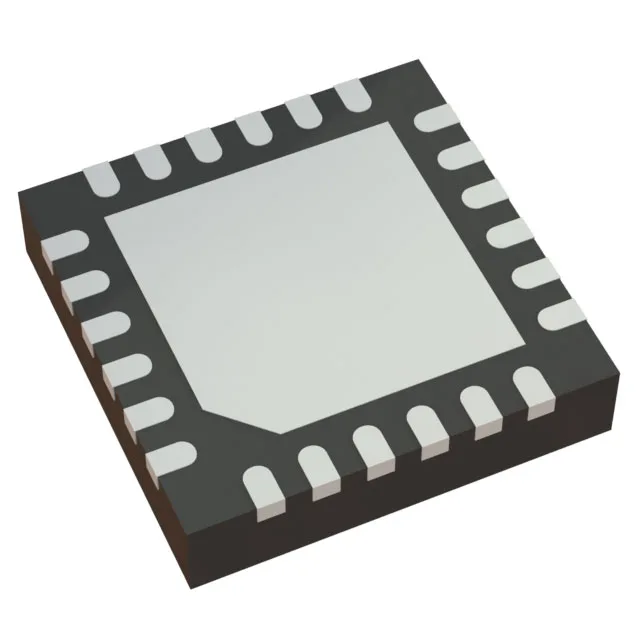
Renesas Electronics RC32504A000GNK#BB0 — Discrete Semiconductors
Technical Documents PDF / CAD
RoHS Compliant · Lead-Free EIA-481 Standard
Renesas Electronics / Discrete Semiconductors

Renesas RC32504A000GNK#BB0 FemtoClock Frequency Translator

MPN RC32504A000GNK#BB0
End of Life Spot Stock · 24-48h Dispatch 100% Original Sealed

Renesas FemtoClock® RC32504A000GNK#BB0, PLL-based Frequency Translator, 2:5 ratio, differential I/O, 180 MHz / 1 GHz max, 1.71V–1.89V / 3.465V supply, -40 to 85°C, 24-VFQFPN (4x4).

In Stock: 1 pcs
MOQ: 1 pcs
Logistics: DHL / FedEx DAP (Global Express · 3-7d) Russia & CIS DDP (Door-to-Door Cleared)
Dispatch: Shenzhen / HK
Unit Price (USD)
$17.04 / pc
Direct Purchase Ready
Volume Pricing Breaks Confirmed upon quotation
1+ pcs
$17.04
Working on a production BOM or have a target unit price? Submit Target Price
Buy Now

$17.04 / ea

1 in stock — maximum per order · 3–4 days lead time

Upload Full BOM List
[SPEC] Essential Parameters Snapshot Full Specifications (15)
Package / Case 24-WFQFN Exposed Pad
Supply Voltage 1.71V ~ 1.89V, 3.465V

Full Technical Specifications

15 Parameters
RC32504A000GNK#BB0 specifications
Parameter / AttributeSpecification / Value
TypeFrequency Translator
SeriesFemtoClock®
MountingSurface Mount
Supply voltage1.71V ~ 1.89V, 3.465V
Frequency - max180MHz, 1GHz
Operating temperature-40°C ~ 85°C (TA)
PLLYes
InputHCSL, LVCMOS, LVDS, Crystal
OutputCML, HCSL, LVCMOS, LVDS, LVPECL
PackageTray
Case24-WFQFN Exposed Pad
Divider (Multiplier)Yes/No
Number of circuits1
Ratio - Input:Output2:5
Differential - Input:OutputYes/Yes
Series Sibling Variants

Renesas Electronics FemtoClock® Series Models

Sibling variants, package options, and speed/density grades in this Renesas Electronics semiconductor series. Active Shenzhen warehouse allocation and rapid 24-48h dispatch.

Technical Details & Description

PLL frequency translator for precision clock trees

The Renesas RC32504A000GNK#BB0 is a FemtoClock® PLL-based frequency translator that accepts HCSL, LVCMOS, LVDS, or crystal inputs and delivers up to five outputs in CML, HCSL, LVCMOS, LVDS, or LVPECL formats. It operates from a 1.71 V to 1.89 V core supply plus a 3.465 V I/O rail, and is rated over the -40°C to 85°C industrial temperature range. This part is designed for clock conditioning in networking, base-station, and FPGA-based systems where jitter cleaning and format conversion are required.

Dual frequency maximums — which one applies

The frequency maximum is listed at both 180 MHz and 1 GHz. The 1 GHz figure applies to the differential output paths (CML, LVPECL, LVDS), while the 180 MHz limit governs the LVCMOS single-ended outputs.

Supply sequencing matters

Two separate supply domains — a 1.71 V to 1.89 V core and a 3.465 V I/O rail — mean the board designer must sequence or at least ensure both are clean before the PLL locks.

It is ROHS3 compliant. No official replacement or second-source alternate is recorded — this is the current FemtoClock device for this configuration.

Frequently asked questions

What input and output signal types does the RC32504A000GNK#BB0 support?

The RC32504A000GNK#BB0 accepts HCSL, LVCMOS, LVDS, or crystal inputs and outputs CML, HCSL, LVCMOS, LVDS, or LVPECL. All inputs and outputs are differential-capable.

What is the frequency range of the RC32504A000GNK#BB0?

The RC32504A000GNK#BB0 has a maximum frequency of 1 GHz on differential outputs and 180 MHz on LVCMOS outputs.

RC32504A000GNK#BB0
Verified Allocation
Quote