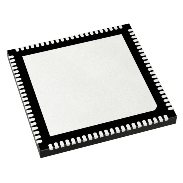
RF sampling clock generator — 6 GHz, 17 outputs, dual reference
The Renesas 8V19N882NVGI is a FemtoClock-series clock generator and jitter attenuator built around an integrated PLL. It accepts LVCMOS, LVDS, or LVPECL reference inputs and delivers up to 17 LVDS or LVPECL outputs at frequencies up to 6 GHz — a part aimed directly at RF sampling ADC/DAC clock trees, high-speed data converter front-ends, and instrumentation backplanes where phase noise floor determines system SNR. The 2:17 input-to-output ratio means two reference inputs feed a bank of 17 synthesized outputs. That buys you redundant reference switching without an external mux — one input can be a clean local oscillator, the other a system reference, with hitless switching managed inside the device. Supply voltage is split across three ranges: 1.7 V to 1.9 V, 2.4 V to 2.6 V, and 3.2 V to 3.4 V. The core, PLL, and output banks each have their own supply domain.
No NRND or last-time-buy flags — this part is current-production and intended for new designs. The FemtoClock family is Renesas' high-performance clocking portfolio, so ongoing support and future spin compatibility are expected.