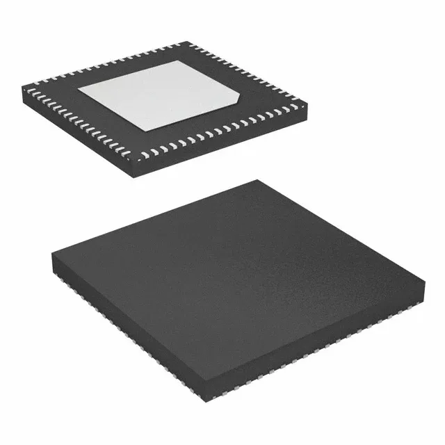
Universal frequency translator for multi-standard clock trees
The Renesas 8T49N286A-999NLGI is a FemtoClock® NG PLL-based frequency translator that accepts HCSL, LVCMOS, LVDSM, LVHSTL, LVPECL, or crystal inputs and delivers HSCL, LVCMOS, LVDS, or LVPECL outputs. With a maximum output frequency of 1 GHz and a 5:8 input-to-output ratio, it serves as a single-chip clock distribution and format-conversion point in systems that need to bridge multiple signalling standards — common in telecom line cards, FPGA reference-clock trees, and high-speed data-acquisition front-ends.
1 GHz ceiling and the timing margin it buys
The 1 GHz maximum output frequency covers reference clocks for high-speed SerDes, ADCs, and FPGAs. The PLL-with-bypass mode routes a clean external clock through when the on-chip PLL is not needed.
Input and output flexibility reduces BOM count
Supporting six input types (HCSL, LVCMOS, LVDSM, LVHSTL, LVPECL, Crystal) and four output types (HSCL, LVCMOS, LVDS, LVPECL) means a single 8T49N286A-999NLGI can replace multiple dedicated translators on a mixed-standard board. The differential input and output capability (Yes/Yes) keeps signal integrity intact over longer board traces or backplane runs.
The supply range of 2.375 V to 3.465 V covers common mixed-signal rails.