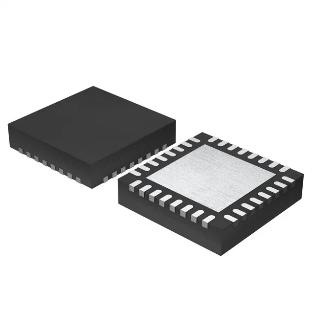
Renesas Electronics 8T49N004A-999NLGI — Clock & Timing ICs
Technical Documents PDF / CAD
RoHS Compliant · Lead-Free EIA-481 Standard
Renesas Electronics / Clock & Timing ICs

8T49N004A-999NLGI FemtoClock NG PLL Clock Generator

MPN 8T49N004A-999NLGI
End of Life Spot Stock · 24-48h Dispatch 100% Original Sealed

Renesas (IDT) FemtoClock® NG PLL clock generator, 8T49N004A-999NLGI, 200 MHz max LVPECL output, 1:4 fanout, crystal input, 2.375V–3.465V supply, -40 to 85°C, 32-VFQFN exposed pad.

In Stock: 490 pcs
MOQ: 1 pcs
Logistics: DHL / FedEx DAP (Global Express · 3-7d) Russia & CIS DDP (Door-to-Door Cleared)
Dispatch: Shenzhen / HK
Unit Price (USD)
$17.14 / pc
Direct Purchase Ready
Volume Pricing Breaks Confirmed upon quotation
1+ pcs
$17.14
10+ pcs
$15.43
30+ pcs
$14.05
100+ pcs
$12.68
Working on a production BOM or have a target unit price? Submit Target Price
Buy Now

$17.14 / ea

490 in stock — maximum per order · 3–4 days lead time

$15.43 / ea from 10 pcs

Upload Full BOM List
[SPEC] Essential Parameters Snapshot Full Specifications (14)
Package / Case 32-VFQFN Exposed Pad
Supply Voltage 2.375V ~ 3.465V

Full Technical Specifications

14 Parameters
8T49N004A-999NLGI specifications
Parameter / AttributeSpecification / Value
SeriesFemtoClock® NG
MountingSurface Mount
Supply voltage2.375V ~ 3.465V
Frequency - max200MHz
Operating temperature-40°C ~ 85°C
PLLYes with Bypass
InputCrystal
OutputLVPECL
PackageTray
Case32-VFQFN Exposed Pad
Divider (Multiplier)Yes/No
Number of circuits1
Ratio - Input:Output1:4
Differential - Input:OutputNo/Yes
Series Sibling Variants

Renesas Electronics FemtoClock® NG Series Models

Sibling variants, package options, and speed/density grades in this Renesas Electronics semiconductor series. Active Shenzhen warehouse allocation and rapid 24-48h dispatch.

Technical Details & Description

200 MHz LVPECL output — what it buys you

The 200 MHz maximum output frequency on LVPECL pairs well with high-speed SERDES reference clocks, FPGA transceiver reference clocks, or Ethernet PHY master clocks. LVPECL gives you fast edge rates and good noise margin on differential lines, but it also means the termination network matters — plan for Thevenin-equivalent or AC-coupled termination at the receiver. The 1:4 fanout lets one crystal feed four clock domains without an external fanout buffer, saving board space and part count.

Lifecycle and sourcing — active, no end-of-life pressure

Frequently asked questions

What is the output frequency range of 8T49N004A-999NLGI?

The maximum output frequency is 200 MHz on the LVPECL outputs. The lower end is set by the crystal input frequency and the PLL divider range; with a typical 25 MHz crystal, the PLL can synthesize down to sub-MHz rates.

Is 8T49N004A-999NLGI compatible with 3.3V supply?

Yes, the supply range is 2.375 V to 3.465 V, which comfortably covers 3.3 V ±10%. It also works on 2.5 V rails.

Does 8T49N004A-999NLGI have an exposed pad?

Yes, the 32-VFQFN package includes an exposed pad (5x5 mm) that serves as both thermal relief and ground connection. The pad must be soldered to the PCB ground plane for proper thermal and electrical performance.

Can 8T49N004A-999NLGI be used with a 25 MHz crystal?

Yes, the input accepts a crystal, and a 25 MHz fundamental-mode crystal is a common choice for this PLL. The internal oscillator and PLL will lock to the crystal frequency and multiply it up to the desired output rate within the 200 MHz limit.

What is the closest pin-compatible alternative to 8T49N004A-999NLGI?

Within the FemtoClock® NG family, the 8T49N004A-999NLGI is a specific variant with LVPECL output and 1:4 fanout. Other family members share the same 32-VFQFN footprint but may differ in output logic (LVDS, HCSL) or fanout ratio. Check the Renesas FemtoClock® NG selector guide for exact pin-compatible drop-ins; the datasheet pinout table is the definitive reference.

8T49N004A-999NLGI
Verified Allocation
Quote