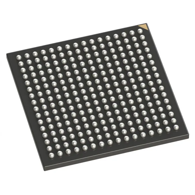
Lattice Semiconductor LFCPNX-100-7ASG256C — FPGA / CPLD & Programmable Logic

LFCPNX-100-7ASG256C FPGA – 96K LEs, 169 I/O, CertusPro-NX

MPNLFCPNX-100-7ASG256C
Active

Lattice Semiconductor CertusPro™-NX FPGA, order code LFCPNX-100-7ASG256C, 96,000 logic elements, 169 user I/O, 3.8 Mbit block RAM, 0.95 V core, 256-ball WLP, commercial temp 0°C to 85°C.

$77.29Ref. price · indicative, final on quote
Independent supplier — new & surplus stockAuthenticity-screened · ESD-safe packingListing updated Aug 2026

Specifications

LFCPNX-100-7ASG256C specifications
ParameterValue
SeriesCertusPro™-NX
MountingSurface Mount
Operating temperature high0°C to 85°C (TJ)
Package_typeTray
Number of i (O)169
Total ram bits3833856
StatusActive
Supply voltage0.95
Number of labs (Clbs)24000
Number of logic elements (Cells)96000

Product details

96,000 logic elements – what fits in the fabric

The LFCPNX-100-7ASG256C packs 96,000 logic elements organised as 24,000 LABs/CLBs – enough for a soft-core RISC-V processor plus a video scaler and a few SPI/I2C peripherals without spilling into a larger package. The 169 user I/O in a 256-ball WLP means every ball that is not a power/ground pin is a signal; plan the fan-out early because the 0.95 V core rail needs a dedicated regulator and decoupling right under the package.

3.8 Mbit block RAM – buffer budget

On-chip block RAM totals 3,833,856 bits, which is roughly 480 KB. That is enough for a 640×480 frame buffer at 8-bit depth or a moderate packet FIFO. If the application needs more than this, the 169 I/O can drive an external DDR3 or SDRAM bus – but the board will need the extra memory device and its supply rails.

That is a commercial-grade envelope – fine for office equipment, test gear, or indoor networking. Not rated for engine-bay, outdoor base-station, or military ambient. If the BOM calls for industrial or automotive temp, the sibling LFCPNX-100-8CBG256C shares the same logic density but check its temp grade separately; the 'C' suffix here signals commercial.

The CertusPro-NX family is current-generation silicon, so allocation risk is low through standard distribution.

Frequently asked questions

Is LFCPNX-100-7ASG256C obsolete or still active?

Active. Lattice Semiconductor lists this order code as Active with no PCN or EOL notice. No successor has been announced because the part is current-generation.

What is the logic capacity of LFCPNX-100-7ASG256C?

96,000 logic elements arranged as 24,000 LABs/CLBs. This is the same logic fabric as the sibling LFCPNX-100-7CBG256C – the difference is the package and the speed grade.

When sourcing LFCPNX-100-7ASG256C, what is the closest functional second-source?

The LFCPNX-100-7CBG256C is the closest sibling: same 96,000 logic elements, same 169 I/O, same 3.8 Mbit block RAM, same 0.95 V core. The difference is the package – 7CBG256C is a 256-ball caBGA vs the 7ASG256C's 256-ball WLP. If the board footprint allows a BGA, the 7CBG256C is a direct parametric match.

Does LFCPNX-100-7ASG256C require external configuration memory?

The evidence does not specify internal configuration memory details. CertusPro-NX FPGAs typically use on-chip flash for non-volatile configuration, but confirm the exact boot method from the full datasheet – the block RAM is for user data, not configuration storage.