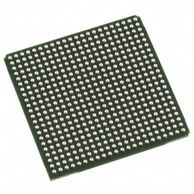
Lattice Semiconductor LFXP2-40E-5FN484C — FPGA / CPLD & Programmable Logic

Lattice LFXP2-40E-5FN484C FPGA, 40K LEs, 363 I/O, 484FBGA

MPNLFXP2-40E-5FN484C
Active

Lattice Semiconductor XP2 series FPGA, LFXP2-40E-5FN484C, 40000 logic cells, 363 I/O, 906240 total RAM bits, 1.14 V core, 484-ball FBGA, tray.

$158.45Ref. price · indicative, final on quote
Independent supplier — new & surplus stockAuthenticity-screened · ESD-safe packingListing updated Aug 2026

Specifications

LFXP2-40E-5FN484C specifications
ParameterValue
SeriesXP2
MountingSurface Mount
Operating temperature high0°C to 85°C (TJ)
Package_typeTray
Number of i (O)363
Total ram bits906240
StatusActive
Supply voltage1.14
Number of labs (Clbs)5000
Number of logic elements (Cells)40000

Product details

40K logic cells, 363 I/O — XP2 mid-range FPGA

The LFXP2-40E-5FN484C is a Lattice Semiconductor XP2-series FPGA delivering 40000 logic cells and 363 user I/O in a 484-ball FBGA package. On-chip block RAM totals 906240 bits, and the device is built around 5000 LUT-4-based logic slices (Labs/CLBs) — enough for moderate-complexity glue logic, bridge functions, or a soft-core MCU peripheral set.

Frequently asked questions

How do I get current pricing and availability for LFXP2-40E-5FN484C?

Submit an RFQ against your target quantity.

When sourcing LFXP2-40E-5FN484C, what's the closest functional alternative — LFE3-35EA-6FN484C?

The LFE3-35EA-6FN484C is a higher-density ECP3-series sibling with 33000 logic cells, 295 I/O, and 1358848 bits of block RAM. It is not pin-compatible — the 484FBGA footprint differs in ball assignment — so a board spin is required to swap. For a drop-in replacement within the same package, stay with the XP2 family; the LFXP2-40E-5FN484C is the largest I/O-count variant in that series.