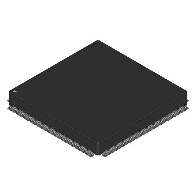
Lattice Semiconductor OR2T40A6PS240-DB — FPGA / CPLD & Programmable Logic

Lattice OR2T40A6PS240-DB ORCA™2 FPGA, 184 I/O, 99.4K gates

MPNOR2T40A6PS240-DB
Active

Lattice Semiconductor ORCA™2 FPGA, Bulk package, 184 I/O, 57.6 Kbit RAM, 99.4K gates, 3600 logic cells, 3 V supply, 0°C to 70°C, Surface Mount.

$94.93378Ref. price · indicative, final on quote
Sourced new & surplus through independent channelsAuthenticity-screened · ESD-safe packingListing updated Aug 2026

Specifications

OR2T40A6PS240-DB specifications
ParameterValue
SeriesORCA™2
MountingSurface Mount
Operating temperature high0°C to 70°C(TA)
Package_typeBulk
Number of i (O)184
Total ram bits57600
StatusActive
Number of gates99400
Supply voltage3.0
Number of logic elements (Cells)3600

Product details

What the 184 I/O and 99.4K gates mean for a board fit

The OR2T40A6PS240-DB is a Lattice Semiconductor ORCA™2 FPGA with 184 user I/O, 99,400 usable gates, and 3,600 logic cells — the I/O count is the first constraint for a board-level route: 184 signals need fan-out across several layers on a dense PCB, and the 3 V supply rail simplifies the power tree by eliminating a separate 1.8 V or 2.5 V core rail. The 57.6 Kbit on-chip RAM is sized for small FIFO buffers or register files, not large frame stores — anything beyond a few hundred bytes of local storage pushes the design to external SRAM or SDRAM.

Frequently asked questions

What is the on-chip memory capacity of this FPGA?

The OR2T40A6PS240-DB has 57.6 Kbit of total RAM bits — enough for small FIFO buffers, register files, or configuration shadowing, but not for large frame stores or packet buffers without external memory.