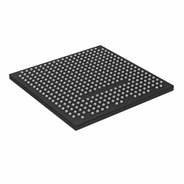
44,000 logic elements in a 17x17 mm BGA
The LFE5UM5G-45F-8BG381I is a mid-density ECP5-5G FPGA from Lattice Semiconductor, packing 44,000 logic elements and 203 user I/O into a 381-ball CABGA package measuring 17x17 mm. The 1,990,656 total RAM bits give you block memory for FIFOs, line buffers, or small packet caches without reaching for external SRAM.
Industrial temperature grade and narrow core supply
The core supply window is tight — 1.045V to 1.155V — so the board's voltage regulator needs ±3% accuracy or better to stay inside the operating envelope. The 1.045V minimum means a standard 1.2V rail with 5% tolerance (1.14V min) is too low; plan for a programmable or adjustable regulator. The 203 I/O count in a 381-ball BGA leaves about 178 balls for power, ground, and configuration — typical for a mid-range FPGA where signal-to-ground ratio is around 1.1:1. The 0.8 mm ball pitch on the 17x17 mm body routes cleanly on a 6-layer board with microvias; an 8-layer stack gives you a dedicated ground plane under the core.
Active production with ROHS3 compliance
This is a current-production part you can design into new builds without worrying about a near-term EOL.
Pin-compatible peer for speed-grade swaps
The LFE5UM-45F-7BG381I shares the same 203 I/O, 381-CABGA package, 44,000 logic elements, and 1,990,656 RAM bits — the only difference is the speed grade (7 vs 8). If your timing closure passes on the -7 grade, the -8 gives you extra margin; if you have -7 stock and need -8 performance, the BOM swap is a direct drop-in without a board spin.