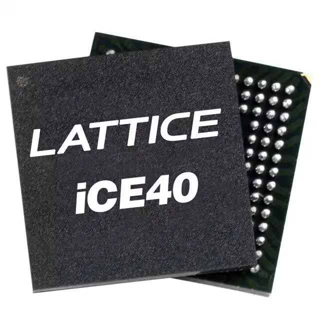
Package and board-fit — 36-UCBGA, 2.5 x 2.5 mm
The ICE40LP1K-CM36A ships in a 36-VFBGA package (supplier device package 36-UCBGA, 2.5 x 2.5 mm) with 25 user I/O. The 0.5 mm ball pitch and small footprint demand a controlled-impedance PCB stack-up and a stencil designed for fine-pitch BGA assembly — the board layout engineer should budget for micro-via fan-out under the package.
Logic fabric and on-chip memory
The device integrates 1280 logic cells (160 LABs/CLBs) and 65536 total RAM bits. For a glue-logic or sensor-interface design, the 1280 LEs handle simple state machines and data-path muxing while the 64 Kbit block RAM buffers small FIFOs or look-up tables — the memory headroom is tight for anything beyond a few hundred bytes of buffering.
Supply voltage and temperature grade
Core supply is 1.14 V to 1.26 V, a narrow window that requires a regulated rail — a standard 1.2 V LDO with ±2 % tolerance keeps the FPGA within spec.
Lattice Semiconductor lists the ICE40LP1K-CM36A as Active. It is ROHS3 compliant.