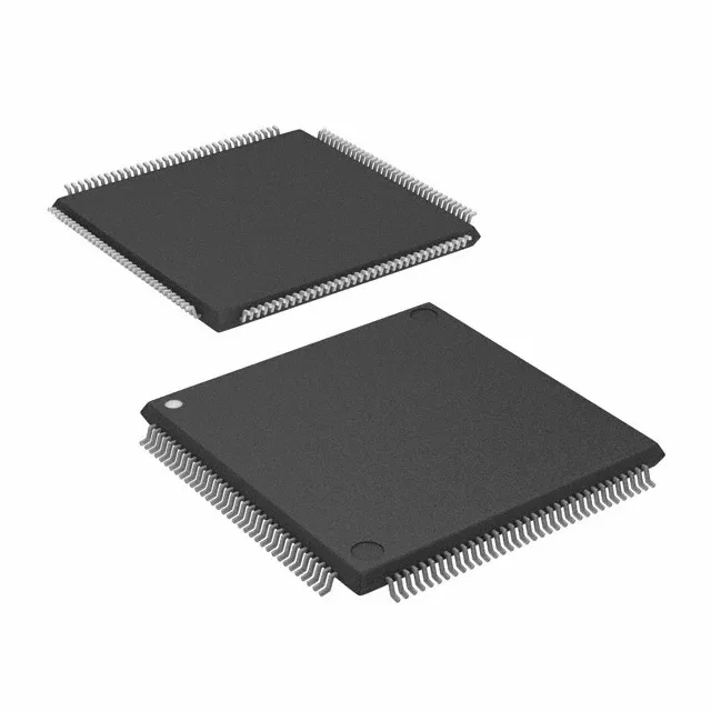
Lattice Semiconductor Corporation ICE40HX1K-TQ144 — FPGA / CPLD & Programmable Logic
Technical Documents PDF / CAD
RoHS Compliant · Lead-Free EIA-481 Standard
Lattice Semiconductor Corporation / FPGA / CPLD & Programmable Logic

ICE40HX1K-TQ144 Lattice iCE40 HX FPGA, 1280 LEs, 96 I/O

MPN ICE40HX1K-TQ144
Active Spot Stock · 24-48h Dispatch 100% Original Sealed

Lattice Semiconductor Corporation iCE40™ HX FPGA, ICE40HX1K-TQ144, 1280 logic elements, 96 I/O, 64 Kbit RAM, 144-LQFP tray, surface mount, 1.14V-1.26V core, -40°C to 100°C.

In Stock: 4 pcs
MOQ: 1 pcs
Logistics: DHL / FedEx DAP (Global Express · 3-7d) Russia & CIS DDP (Door-to-Door Cleared)
Dispatch: Shenzhen / HK
Unit Price (USD)
$15.12 / pc
Direct Purchase Ready
Volume Pricing Breaks Confirmed upon quotation
1+ pcs
$15.12
Working on a production BOM or have a target unit price? Submit Target Price
Buy Now

$15.12 / ea

4 in stock — maximum per order · 3–4 days lead time

Upload Full BOM List
[SPEC] Essential Parameters Snapshot Full Specifications (10)
Package / Case 144-LQFP
Supply Voltage 1.14V ~ 1.26V
ALT
Facing long factory lead times or allocation on ICE40HX1K-TQ144? Verified pin-compatible alternatives available with active Shenzhen stock and 100% solder-ready footprint match.

Full Technical Specifications

10 Parameters
ICE40HX1K-TQ144 specifications
Parameter / AttributeSpecification / Value
SeriesiCE40™ HX
MountingSurface Mount
Supply voltage1.14V ~ 1.26V
Operating temperature-40°C ~ 100°C (TJ)
PackageTray
Number of i (O)96
Case144-LQFP
Total RAM bits65536
Number of LABs (CLBs)160
Number of logic elements (Cells)1280
100% Footprint Match · Solder-Ready (No PCB Redesign Needed)

Need Stock or a Drop-in Second-Source for ICE40HX1K-TQ144?

Package: QFN / ucBGA / WLCSP / TQFP · Pin-compatible replacements with immediate Shenzhen spot stock

Footprint Match 97%
Supply Chain & Allocation Reality:

The iCE40 line is the FPGA family that the hobby and small-batch world actually uses - and the data says the same thing about buyers: searches concentrate on Lattice CPLD and iCE40 class parts while Xilinx orderables sit at the noise floor. The family is five sub-splits with wildly different capabilities (UltraLite to UltraPlus) sharing a naming theme and a common trait: an SRAM fabric that must be loaded at every power-up - from an external SPI flash, a host CPU, or the family-internal NVCM. The sourcing consequence is structural: an iCE40 socket is never just an FPGA line on the BOM; it is a two-part relationship with a configuration memory.

Verified Pin-Compatible Replacements (3 verified alternatives)

iCE40UP5K Lattice Semiconductor QFN-48 / SG48 / WLCSP
Functional Equivalent
Availability & Target Pricing:

The UltraPlus Flagship

Shenzhen Spot Stock (24-48h Dispatch)

Electrical & Core Specs:

The richest sub-split: 5,280 LUTs with 1Mb of SPRAM (four 256kb blocks), DSP blocks, two hardened SPI and two I2C blocks, and on-chip oscillators - built for always-on sensor buffering and audio pre-processing.

Low-power single-rail design point; the UltraPlus is the part behind most current iCE40 designs.

Compatibility & Drop-In Notes: Sub-splits are not interchangeable: LP/HX/Ultra/UltraLite/UltraPlus differ in logic, memory and hardened IP. Replacing one with another is a re-synthesis and placement project, and the pin maps differ even in the same package size.
Package & Solder Footprint: Common QFN-48-class outlines are shared - verify pin map against the exact device, not the package.
Shenzhen Warehouse Stock & MOQ: Stocked with config flash paired on request (W25Q-class SPI flash sourced on the same order).
iCE40HX1K Lattice Semiconductor TQFP-144 / VQFP-100 / QFN
Functional Equivalent
Availability & Target Pricing:

The Performance Sub-Split

Shenzhen Spot Stock (24-48h Dispatch)

Electrical & Core Specs:

The HX line trades standby current for more logic per die (HX1K/4K/8K against LP1K/4K/8K); the classic hobby board part of the iCE40 generation.

Low-power but not the micropower LP class; check the static current against the design budget.

Compatibility & Drop-In Notes: LP and HX are the two faces of the same generation: the pin maps match within a device size, but the power and clocking characteristics differ. In repair of hobby-era boards, match the exact device.
Package & Solder Footprint: Larger through-hole-friendly VQFP/TQFP outlines exist in this line.
Shenzhen Warehouse Stock & MOQ: Stocked for repair of the hobby and education ecosystem boards.
ECP5 Lattice Semiconductor caBGA / csBGA families
Functional Equivalent
Availability & Target Pricing:

The Step-Up Platform

Shenzhen Spot Stock (24-48h Dispatch)

Electrical & Core Specs:

The next class above iCE40 in the Lattice stack: higher logic density and hardened high-speed interfaces for video, networking and instrumentation designs.

Multi-rail FPGA supply design - not a drop-in to any iCE40 socket.

Compatibility & Drop-In Notes: Listed to complete the Lattice map - the two families share tooling (Lattice Radiant) but nothing electrical. The honest cross-family statement: re-design, not replacement.
Package & Solder Footprint: BGA-only packaging; assembly and inspection requirements differ from iCE40 QFN work.
Shenzhen Warehouse Stock & MOQ: Stocked per part number with photographed markings - BGA FPGAs are a favored relabeling target.
Buyer & Quality Checklist for Sourcing Alternatives
  • Every iCE40 is SRAM-based: the design lives in configuration memory loaded at power-up (external SPI flash, host controller, or NVCM where present). A board without its config flash is a board with a blank FPGA - when sourcing iCE40, source the paired W25Q-class flash on the same order.
  • The five sub-splits (UltraLite / LP / HX / Ultra / UltraPlus) are different devices, not grades of one device: logic, memory, DSP and hardened IP differ, and the same-size package does not imply the same pin map.
  • Small packages drop features: several mini outlines have no PLL, and the constant-current LED sink exists on selected packages only. The package letter in the orderable number is a spec, not a shipping choice.
  • NVCM configurations are instant-on and secure but one-shot - production planning for NVCM-programmed devices needs lead time and programming decisions upstream, not at the bench.
  • The market leans Lattice for this class (buyer searches concentrate here, not on Xilinx orderables): keep depth in iCE40 and the config flash, with ECP5 quoted case-by-case.
  • iCE40 boards in the repair channel are numerous (hobby, education, instrumentation): the two failure parts are the FPGA and its config flash - check the flash first, it is cheaper and it holds the bitstream.
Frequently Asked Technical Questions

Q: Which iCE40 sub-family do I need?

A: Choose by need: UltraPlus (UP5K) when on-chip SPRAM or DSP is required; HX/LP for general low-power logic with more density; Ultra for mobile glue logic with hardened SPI/I2C; UltraLite for the absolute smallest always-on designs. Sub-splits are not interchangeable.

Q: Does iCE40 need an external flash chip?

A: It configures at every power-up: from an external SPI flash in self-boot mode, from a host CPU in slave mode, or from the internal NVCM where the design was programmed there. Most boards carry a small W25Q-class SPI flash for the bitstream - source it with the FPGA.

Q: Can I replace a dead iCE40 with an ECP5?

A: No - different family, different packaging and supply design. ECP5 is the step-up platform for higher density and interfaces; migrating is a re-layout and re-synthesis project.

Technical Details & Description

Logic density and I/O — what 1280 LEs and 96 I/O mean for a glue-logic FPGA

The ICE40HX1K-TQ144 packs 1280 logic elements (160 LABs/CLBs) and 64 Kbit of block RAM, enough to absorb a handful of 8-bit counters, a small state machine, and a SPI bridge without leaving the iCE40 HX family's low-power envelope. 96 user I/O in a 144-TQFP (20x20 mm) means every available pin on the package is an I/O — no power-dedicated pins beyond the core and PLL supplies — so the pinout is dense and the board layout needs to account for the 1.14 V to 1.26 V core rail being clean within 50 mV.

Tray packaging means the devices are delivered in antistatic trays, not tape-and-reel — a pick-and-place machine can handle trays, but the feeder setup differs from reel-fed lines.

Active lifecycle and compliance — no LTB risk on this code

ROHS3 compliant and the base part number ICE40 covers the whole iCE40 family, so the same compliance documentation applies across the HX and LP variants.

Frequently asked questions

What is the closest alternative to ICE40HX1K-TQ144 — the ICE40HX1K-CB132?

The ICE40HX1K-CB132 shares the same logic fabric (1280 LEs, 64 Kbit RAM) and temperature range, but uses a 132-ball caBGA package with 95 I/O instead of 96. The BGA footprint is not pin-compatible with the 144-TQFP — a board spin is required to swap between them.

ICE40HX1K-TQ144
Verified Allocation
Quote