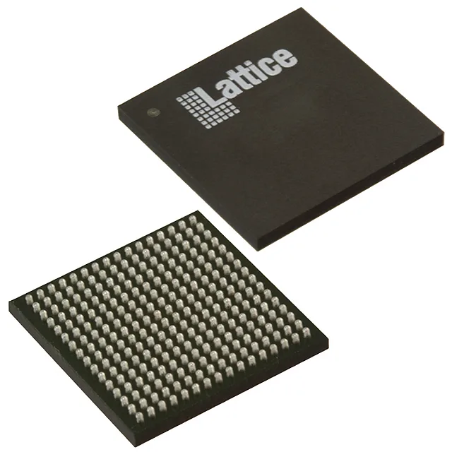
6864 logic cells in a 9×9 mm BGA — the MachXO3 glue-logic workhorse
The LCMXO3LF-6900E-6MG256C is a Lattice MachXO3 FPGA packing 6864 logic elements (858 LABs/CLBs) and 206 user I/O in a 256-ball CSFBGA measuring 9×9 mm. That 0.5 mm ball pitch means the fan-out fits on a standard 4-layer board without microvias — a practical choice for a bridge or control-logic FPGA that sits between a processor and a set of peripherals. The 245760 bits of embedded block RAM (distributed across the fabric) handle small FIFOs, look-up tables, or line buffers without chewing up logic cells. For a glue-logic design that needs a few hundred flip-flops and a modest state machine, this part leaves headroom for last-minute ECOs.
1.14–1.26 V core — commercial temp, active production
Core supply is 1.14 V to 1.26 V — a tight 120 mV window that demands a regulated rail, not a shared 1.2 V from a buck converter running open-loop. The commercial temperature grade (0°C to 85°C junction) covers most indoor and telecom-rack environments; if your design sees -40°C startup, step to the industrial-temp suffix (LCMXO3LF-6900E-6MG256I).
206 I/O — what the bank structure means for your PCB
The 206 I/O are arranged in multiple banks, each with its own Vccio rail. The 256-ball package gives 206 usable I/O; the remaining balls are power, ground, and configuration pins. Configuration is via JTAG or SPI flash — the MachXO3 boots from an external SPI memory on power-up. The 245760 bits of block RAM are volatile; your design's boot code and look-up tables live in the SPI flash, not on-chip.