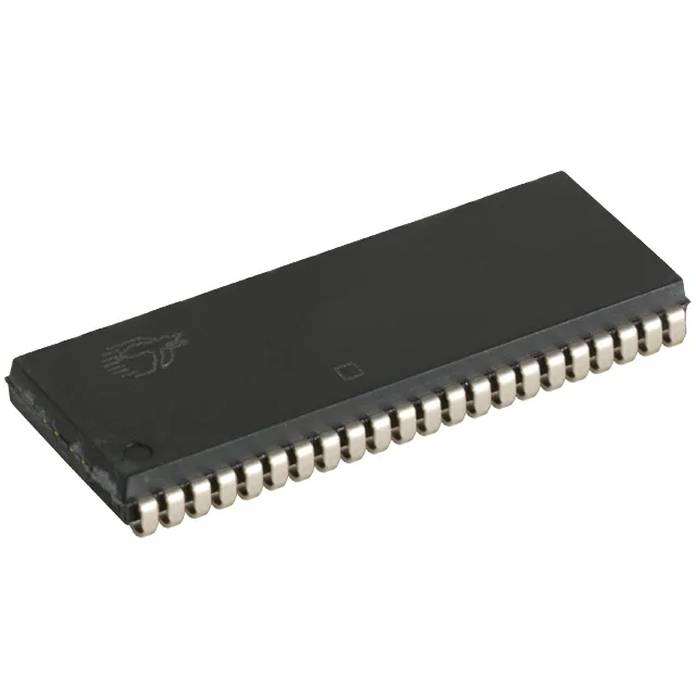
64K x 16 vs 128K x 8 — the bus-width decision
The CY7C1021DV33-10VXI is organized as 64K words by 16 bits, giving a 16-bit data bus on a single chip. The closest sibling, CY7C1018DV33-10VXI, organizes the same 1 Mbit density as 128K x 8 — an 8-bit bus. Both share the 10 ns access time, 3.0-3.6 V supply, and 44-SOJ package, so the choice comes down to whether your memory controller expects a 16-bit or 8-bit data path.
For a 100 MHz bus clock (10 ns period), this leaves zero margin for address-to-data setup in a single-cycle read — you need a wait state or a slower clock domain. In practice, this part is sized for 33-66 MHz controllers where the 10 ns window fits comfortably within a half-cycle or full-cycle read. Write cycle time is also 10 ns, so the write timing matches the read timing — no asymmetric penalty when the controller alternates read and write bursts.
Supply rail and temperature grade
The part is ROHS3 compliant — no exempt phthalates or lead — and ships in tube packaging.
44-SOJ footprint — board-fit note
The 44-SOJ package has a 0.400-inch body width (10.16 mm) with J-bend leads on 1.27 mm pitch. This is a different footprint from TSOP-II or BGA — the solder pads sit under the package body edge, so the land pattern requires a solder mask between pads and a via keep-out zone under the body. If your existing board uses a 44-pin TSOP-II, the SOJ footprint will not drop in without a layout change.