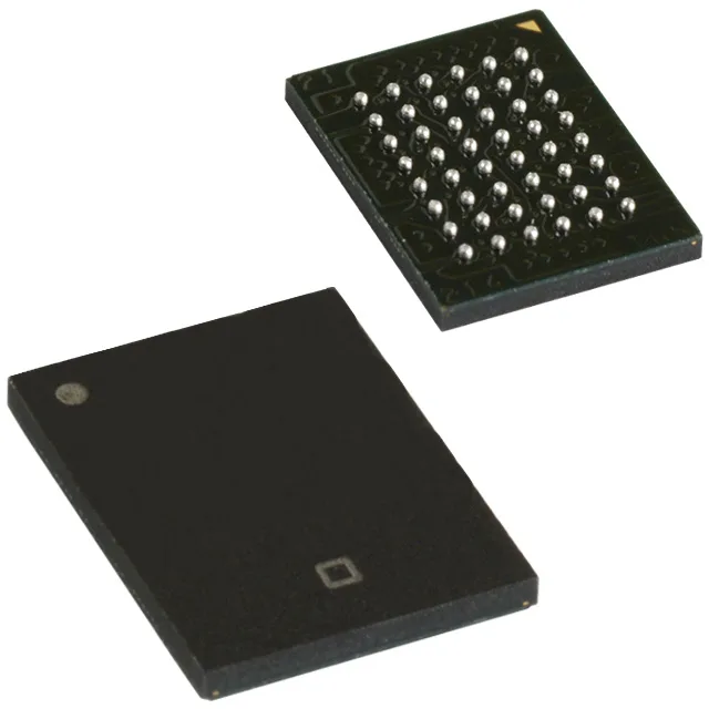
Infineon Technologies CY7C1011DV33-10BVXI — Memory (DRAM / SRAM / Flash / EEPROM)

Infineon CY7C1011DV33-10BVXI SRAM, 2 Mbit, 10 ns, 48-VFBGA

MPNCY7C1011DV33-10BVXI
Active

Infineon Technologies CY7C1011DV33-10BVXI asynchronous SRAM, 2 Mbit (128K x 16), 10 ns access time, parallel interface, 3V-3.6V supply, -40°C to 85°C, 48-VFBGA (6x8 mm), tray.

$4.1900Ref. price · indicative, final on quote
Packaging48-VFBGA
Independent supplier — new & surplus stockAuthenticity-screened · ESD-safe packingListing updated Aug 2026

Specifications

CY7C1011DV33-10BVXI specifications
ParameterValue
Memory typeVolatile
MountingSurface Mount
Voltage3V ~ 3.6V
Memory interfaceParallel
Operating temperature-40°C ~ 85°C (TA)
PackageTray
TechnologySRAM - Asynchronous
Access time10 ns
Memory size2Mbit
Memory formatSRAM
Case48-VFBGA
Memory organization128K x 16
Write cycle time - word, page10ns

Product details

Active 2 Mbit async SRAM in a fine-pitch BGA

The Infineon CY7C1011DV33-10BVXI is an active-production asynchronous SRAM organized as 128K x 16 bits, delivering 2 Mbit of volatile storage with a 10 ns access time. The 10 ns access and write-cycle time sets the bus-margin budget for the memory controller — the data sheet guarantees both read and write at the same 10 ns speed, so the cycle time on the bus is not asymmetric. Housed in a 48-VFBGA (6x8 mm) package, the footprint demands careful PCB layout: the 0.75 mm ball pitch typical for this class of VFBGA requires at least a 4-layer board for fan-out of the 48 balls.

Supply and temperature — single-rail 3.3V with industrial range

Operating from a single 3V to 3.6V supply, the part is a drop-in for 3.3V nominal memory buses common on ARM SoCs, FPGAs, and legacy CPLD-based designs.

Frequently asked questions

What is the memory organization and access time of CY7C1011DV33-10BVXI?

It is a 2 Mbit asynchronous SRAM organized as 128K x 16 bits with a 10 ns access time and 10 ns write-cycle time, both read and write at the same speed.