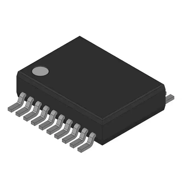
Infineon Technologies CY26580OI-1 — Clock & Timing ICs

CY26580OI-1 Clock Generator, 133.33 MHz, 20-SSOP

MPNCY26580OI-1
End of Life

Cypress Semiconductor PacketClock™ clock generator, fanout distribution, multiplexer, CY26580OI-1, 133.33 MHz max, PLL with bypass, 1:2 I/O, 3.14-3.47 V, -40 to 85°C, 20-SSOP, Bulk.

$1.48Ref. price · indicative, final on quote
Packaging20-SSOP (0.154", 3.90mm Width)
RoHSNot applicable
SeriesPacketClock™
Sourced new & surplus through independent channelsAuthenticity-screened · ESD-safe packingListing updated Aug 2026

Specifications

CY26580OI-1 specifications
ParameterValue
TypeClock Generator, Fanout Distribution, Multiplexer
SeriesPacketClock™
MountingSurface Mount
Voltage3.14V ~ 3.47V
Frequency133.33MHz
Operating temperature-40°C ~ 85°C (TA)
PLLYes with Bypass
InputCMOS
OutputClock
PackageBulk
Case20-SSOP (0.154\", 3.90mm Width)
Divider (Multiplier)Yes/No
Number of circuits1
Ratio - Input:Output1:2
Differential - Input:OutputNo/No

Product details

133.33 MHz PLL clock source with bypass — BOM-fit note

The CY26580OI-1 is a PacketClock™ clock generator that also integrates fanout distribution and a multiplexer in a single 20-SSOP package. Its maximum output frequency of 133.33 MHz sets the clock ceiling for the target interface — typically a SONET/SDH or Ethernet framer that needs a clean reference at that rate. The on-chip PLL includes a bypass mode (: PLL Yes with Bypass), meaning the reference clock can pass through unmodified when the system needs a jitter-free path or during board-level debug. Input and output are both single-ended CMOS, not differential — the fanout stays within a single board, not a backplane. The industrial temperature range (-40°C to 85°C,) suits outdoor telecom cabinets or factory-floor controllers where ambient heat cycles are the norm.

Package and supply integration

The supplier device package is listed as 20-QSOP — the QSOP variant shares the same footprint but has a thinner body; both are surface-mount and reflow-compatible. Single PLL circuit with a 1:2 input-to-output ratio — one reference clock drives two output trees. The divider/multiplier block is present (Yes/No,), so the PLL can multiply the reference up to the 133.33 MHz ceiling or divide it down for lower-speed domains.

Frequently asked questions

What is the PLL configuration on the CY26580OI-1?

The PLL is listed as Yes with Bypass. This means the internal phase-locked loop can be engaged for frequency synthesis or bypassed entirely, letting the reference clock pass through unmodified. Input and output are both single-ended CMOS; there is no differential I/O.