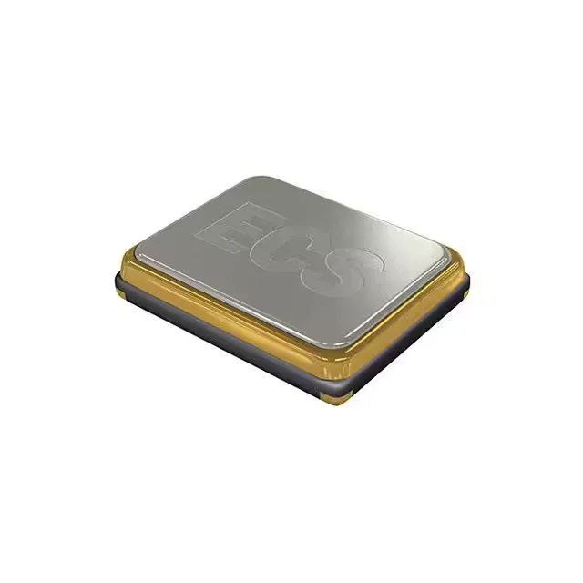
24 MHz fundamental — the timing anchor for USB and CAN designs
The ECS-240-18-33-JEN-TR3: At 24 MHz this sits squarely in the frequency band used for USB Full Speed clocking, SDIO interfaces, and CAN/CAN-FD timing references — the three most common reasons a BOM line lands on this part number.
Tolerance, stability, and ESR — what the numbers mean for timing budget
For a USB 2.0 Full Speed design, the total accumulated drift budget is roughly ±2400 ppm (250 ns full-bit-time tolerance at 12 Mb/s), so this crystal leaves comfortable headroom — the tighter room-temperature tolerance of ±20 ppm is what matters for the initial clock calibration step. Load capacitance is specified at 18 pF. The crystal oscillator circuit must provide this total shunt capacitance at both pins — the PCB trace capacitance, any parasitic, and any external loading capacitors all sum into the tank. Mismatching the load capacitance shifts the actual oscillation frequency away from the 24 MHz nominal, which is why the tolerance spec is measured under the defined load condition, not at some other capacitance value. Equivalent series resistance is 40 Ω maximum. At 24 MHz this ESR level produces a drive-level of roughly 10–20 µW under typical MCU oscillator circuit conditions, well below the crystal's damage threshold. The ESR also sets the startup time constant — a 40 Ω ESR with a typical MCU built-in bias resistor keeps startup within the datasheet limits of most microcontrollers targeting USB or CAN timing.
ECX-32 footprint — what the 3.2 × 2.5 mm package means for layout
The 4-SMD no-lead package uses the standard ECX-32 land pattern. The four terminations are the four corners of the ceramic body — pins 2 and 4 are the crystal connections; pins 1 and 3 are the case ground or no-connect depending on the device variant. The no-lead format reduces lead inductance compared to a gull-wing part at this frequency, which matters for oscillator circuit Q.