Load capacitance and ESR — the two specs that govern oscillator startup
The ECS-184-18-23A-EN-TR: Load capacitance is specified at 18 pF — this is the value the oscillator circuit must present across the crystal terminals for the device to oscillate at its marked frequency. If the actual load presented by the MCU or PLL's internal caps and PCB trace capacitance adds up to something different, the crystal runs off-frequency by roughly the ratio of actual to rated load capacitance squared. Budget the total CL carefully in any low-power or precision timing circuit — the 18 pF figure is not a suggestion, it is the target the circuit designer must hit. Equivalent series resistance is 60 Ω maximum. For a fundamental-mode AT-cut crystal at 18 MHz, this figure is the headroom — the drive-level margin between what the oscillator circuit can supply and what the crystal dissipates at rated drive power. A circuit with marginal startup gain (low-power MCU with a trimmed oscillator bias) can fail to start if the actual ESR creeps above the rated max, particularly after the crystal has been in service for thousands of hours. The 60 Ω spec gives you that headroom to spec against.
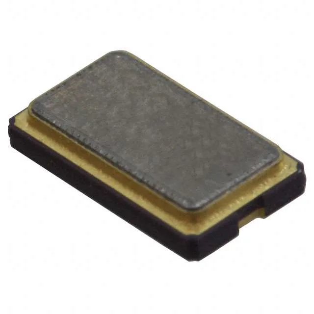
ECX-64A package — footprint and thermal profile for board layout
Land pattern and paste geometry for this package matter more than for through-hole parts: the no-lead configuration means the solder joint is entirely visible from above, which helps inspection but leaves no compliance margin if the pad is slightly oversized. A typical NSMD land for this package runs about 3.40 mm × 1.90 mm per pad; check the ECX-64A datasheet land pattern before releasing the layout. This is not an automotive or extended temperature grade; a design targeting under-hood or outdoor-freezer environments needs a different crystal or a tighter temperature compensation scheme.