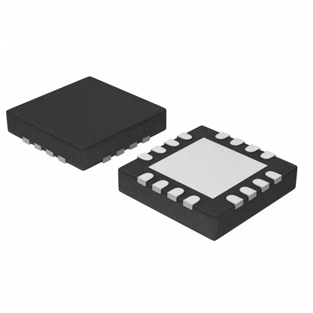
Single-phase synchronous buck controller for point-of-load regulation
The ADP1851ACPZ-R7: It operates from a 2.75 V to 20 V supply rail and switches between 200 kHz and 1.5 MHz, giving the layout engineer flexibility to balance inductor size against switching losses.
What the 90% max duty cycle and synchronous rectification mean for your rail
A 90% maximum duty cycle means the high-side FET can stay on for up to 90% of each switching period — useful when the input voltage is only slightly above the output target, such as regulating 3.3 V from a 3.6 V lithium cell. Synchronous rectification replaces the freewheeling diode with a low-Rds(on) FET, cutting the rectifier drop from ~0.5 V to tens of millivolts; at 5 A output this saves over 2 W of dissipation compared to a non-synchronous design. The output type is Transistor Driver, meaning the chip itself does not integrate the power FETs — it drives external N-channel MOSFETs, so the designer selects FETs sized for the load current and thermal budget.
Control features and clock synchronization for noise-sensitive designs
Control features include current limit, enable, frequency control, power good, ramp, soft start, and tracking — the tracking input lets the output voltage follow another rail during startup, useful for sequencing FPGA core and I/O voltages. Clock sync capability (Yes) allows the switching frequency to lock to an external clock, shifting the switching harmonics away from a sensitive analog band or aligning with another converter's phase to reduce input ripple current. The output configuration is Positive, and the single-phase, single-output design targets point-of-load rails where a dedicated controller for one voltage is simpler than a multi-phase controller with unused phases.
Package and board integration — 16-LFCSP-WQ with exposed pad
The exposed pad carries the ground return for the gate-drive current loop — a poor thermal connection raises junction temperature above the 125°C max, while a poor electrical connection adds inductance that degrades switching waveforms.