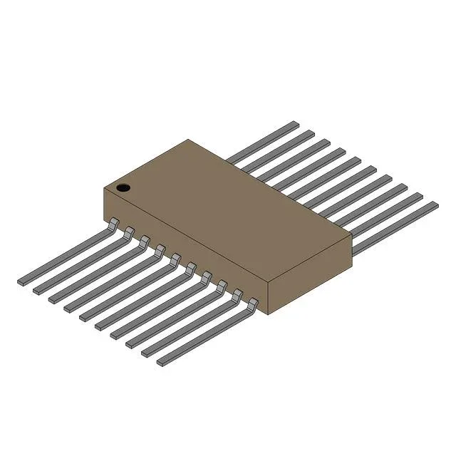
AMD (Xilinx) SN54LS377WB — Logic ICs
Technical Documents PDF / CAD
RoHS Compliant · Lead-Free EIA-481 Standard
AMD (Xilinx) / Logic ICs

SN54LS377WB D-Type Flip-Flop, 40 MHz, 20-CFlatpack

MPN SN54LS377WB
End of Life Spot Stock · 24-48h Dispatch 100% Original Sealed

Texas Instruments SN54LS377WB, D-Type flip-flop, 8-bit, positive-edge triggered, non-inverted outputs, master reset, 40 MHz clock, 4.5 V to 5.5 V supply, -40°C to 125°C, 20-CFlatpack surface-mount package.

In Stock: 1,714 pcs
MOQ: 1 pcs
Logistics: DHL / FedEx DAP (Global Express · 3-7d) Russia & CIS DDP (Door-to-Door Cleared)
Dispatch: Shenzhen / HK
Unit Price (USD)
$12.00 / pc
Direct Purchase Ready
Volume Pricing Breaks Confirmed upon quotation
1+ pcs
$12.00
10+ pcs
$10.80
30+ pcs
$9.84
100+ pcs
$8.88
500+ pcs
$8.28
1,000+ pcs
$7.80
Working on a production BOM or have a target unit price? Submit Target Price
Buy Now

$12.00 / ea

1,714 in stock — maximum per order · 3–4 days lead time

$10.80 / ea from 10 pcs

Upload Full BOM List
[SPEC] Essential Parameters Snapshot Full Specifications (15)
Package / Case 20-CFlatpack
Supply Voltage 4.5V ~ 5.5V
Speed / Frequency 40 MHz
Output / Current 8mA, 400µA

Full Technical Specifications

15 Parameters
SN54LS377WB specifications
Parameter / AttributeSpecification / Value
TypeD-Type
Output typeNon-Inverted
Trigger typePositive Edge
MountingSurface Mount
Supply voltage4.5V ~ 5.5V
Current - quiescent28 mA
Current - output high, low8mA, 400µA
Clock frequency40 MHz
Operating temperature-40°C ~ 125°C (TA)
PackageBulk
FunctionMaster Reset
Case20-CFlatpack
Number of elements1
Number of bits per element8
Max propagation delay @ v, max CL27ns @ 5V, 15pF
[DESK] Shenzhen Spot Allocation · 2h Response

Need Immediate Spot Stock or Shortage Allocation for SN54LS377WB?

Factory lead times blocking production? We lock verified brand-new original stock in Shenzhen within 2 hours.

Quote SLA 2 Hours
[01] Emergency Shortage 24-48h Shenzhen Dispatch

Direct access to Shenzhen floor inventory, franchised allocation buffers, and factory bonded stock to resolve line-down shutdowns.

[02] Industrial Packaging Tape & Reel / Tray / Tube

Standard factory-sealed packaging compliant with EIA-481 standards for automated high-speed SMT pick-and-place lines.

[03] WhatsApp QC Proof 45x Microscope QC Photos

High-resolution photos of original reel labels, 2D DataMatrix, and pin coplanarity sent via WhatsApp/Telegram before you release wire payment.

● USD Wire Transfer (SWIFT T/T) · DAP Express / DDP Delivery

Technical Details & Description

8-bit D-type register with master reset — military-grade bus latch

The SN54LS377WB is an 8-bit D-type flip-flop with master reset, positive-edge triggered, non-inverted outputs. Clock frequency is 40 MHz. Output high is 8 mA, output low is 400 µA.

Clock frequency is 40 MHz. Max propagation delay is 27 ns at 5 V and 15 pF. Quiescent current is 28 mA.

20-CFlatpack — hermetic surface-mount for harsh environments

The 20-CFlatpack is a ceramic, hermetic surface-mount package. Unlike plastic SOIC or TSSOP, the ceramic body resists moisture absorption and thermal shock, making it suitable for military avionics, satellite payloads, downhole tools, and other sealed or high-vibration assemblies. The flat leads require a reflow profile compatible with ceramic — typically a slower ramp rate than plastic packages to avoid thermal stress. Board layout should follow the supplier device package footprint for the 20-CFlatpack; lead pitch is standard for this form factor.

Frequently asked questions

What is the operating temperature range of SN54LS377WB?

The operating temperature range is -40°C to 125°C (TA). This is the military-grade temperature range, suitable for avionics, downhole, and other harsh-environment applications.

Is SN54LS377WB RoHS compliant?

No, the SN54LS377WB is RoHS non-compliant. This is typical for ceramic military-grade packages that use lead-based solder for hermetic seal integrity.

What is the pinout of SN54LS377WB?

The SN54LS377WB is an 8-bit D-type flip-flop in a 20-CFlatpack. Pin assignments follow the standard 54LS377 pinout: clock (pin 1), master reset (pin 13), data inputs D0–D7 (pins 3, 4, 7, 8, 13, 14, 17, 18), and non-inverted outputs Q0–Q7 (pins 2, 5, 6, 9, 12, 15, 16, 19). VCC is pin 20, GND is pin 10. Refer to the TI datasheet for the exact pin diagram.

SN54LS377WB
Verified Allocation
Quote