High-speed signal chain ceiling
The THS4303RGTT is a single-channel general-purpose operational amplifier with a -3dB bandwidth of 1.8 GHz and a slew rate of 5500 V/µs — these two numbers together define the maximum signal frequency and the large-signal rise time the part can handle without distortion. With a gain-bandwidth product of 1.8 GHz, the usable closed-loop bandwidth at a gain of 10 is roughly 180 MHz, making this part a candidate for driving high-speed ADCs, video distribution, or pulse amplification where settling time matters.
Package and thermal layout
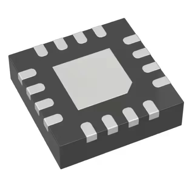
Housed in a 16-VFQFN exposed pad package (3x3 mm body, supplier device package 16-VQFN), the part requires a thermal pad on the PCB for heat sinking — the exposed pad must be soldered to a copper plane to keep the junction temperature within the -40°C to 85°C operating range. The 16-VFQFN footprint is common for high-speed amplifiers; the 3x3 mm body fits tight channel spacing in multi-channel receiver or instrumentation boards.
Power budget and output drive
Supply current is 34 mA per channel, and the output can source or sink up to 180 mA — the 34 mA quiescent draw is modest for a 1.8 GHz amplifier, but the output current capability means it can drive 50-ohm terminated lines or capacitive loads without an external buffer. Operating from a single supply span of 3 V to 5 V, the part fits standard 3.3 V or 5 V rails common in mixed-signal systems; the 1.5 mV typical input offset voltage keeps DC errors low in precision paths.
Lifecycle and compliance
Sourced through authorized and independent distribution channels; quoted to order against the BOM quantity with pricing and lead time confirmed at RFQ.