Triple 3-input NAND in the 4000B family
The CD4023BE is a triple 3-input NAND gate from Texas Instruments' 4000B series, packaged in a 14-pin DIP for through-hole assembly. It integrates three independent NAND gates, each with three inputs, on a single monolithic IC. The 3V to 18V supply range covers standard 5V, 12V, and 15V rails used in industrial control and instrumentation — no separate level translator needed when interfacing with older TTL or higher-voltage CMOS peripherals.
Temperature grade and quiescent current
Quiescent current is 1 µA maximum across the supply range, meaning the gate's own draw is negligible in battery-backed or energy-harvesting designs — the standby power budget is set by the load, not the logic. Output drive is specified at 3.4 mA source and 3.4 mA sink at 15V — enough to switch a standard LED indicator or drive the input of a following CMOS stage, but not intended for heavy loads like relays or solenoids without a buffer.
Propagation delay and switching performance
Maximum propagation delay is 90 ns at 15V with a 50 pF load — this sets the data-rate ceiling for the gate in a signal path. Input logic levels are ratiometric with the supply: low is 1.5V to 4V, high is 3.5V to 11V at VDD=15V. This means the gate interprets a 5V TTL output as a valid high at 15V supply, but at 5V supply the same 5V signal may not reach the high threshold — confirm the supply voltage against the driving stage's output levels.
Package and board integration
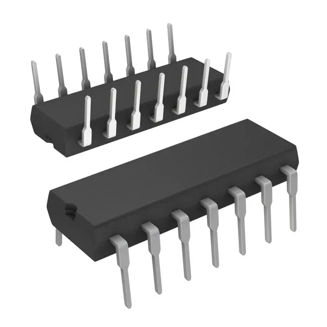
Housed in a 14-DIP (0.300-inch body width, 7.62 mm) with 0.100-inch pin pitch, the CD4023BE fits standard through-hole PCB layouts and breadboard prototyping. The 14-PDIP supplier package is the same footprint used across the 4000B logic family, so a single board layout can accommodate multiple gate functions. Supplied in a tube — the standard DIP shipping format for manual insertion or tube-fed auto-insertion machines. No moisture sensitivity level (MSL) concern for through-hole DIP packages; no bake required before soldering.