Boost regulator with 9-channel current drive
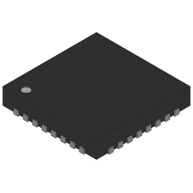
The LP3936SLX is a Texas Instruments DC-DC boost regulator LED driver with nine independent current sinks, each rated 25 mA continuous and 120 mA in flash mode. The internal switching FET runs at 1 MHz, which keeps the external inductor small enough for a compact layout in the 32-TLGA (4.5×5.5 mm) package.
The 25 mA per channel covers typical backlight strings for small-to-medium LCD panels — think phone or portable-instrument displays. The 120 mA flash mode is a separate current path for camera LED flash, not a derated continuous output; the part switches between the two modes based on the PWM control signal. The fixed 5.3 V output rail means no external feedback divider is needed — the boost loop regulates to that voltage, and each channel sinks its programmed current from the LED string. PWM dimming is handled through a dedicated input, so the LED current is chopped at a duty cycle the host processor sets. The 1 MHz switching frequency places the fundamental ripple well above the audible band and lets the output capacitor be a 1 µF ceramic without excessive ripple.
Board integration — package and thermal
The 32-TLGA (4.5×5.5 mm) package has an exposed thermal pad on the bottom. The 0.5 mm pitch land pattern is standard for LGA packages; a 4-layer board with thermal vias under the pad is the typical recommendation for dissipating the boost switch losses. Input supply range is 3 V to 6 V — a single Li-ion cell (3.0–4.2 V) or a 5 V USB rail both work. The internal switch is rated for the boost voltage, so no external Schottky catch diode is needed; the part integrates the rectifier.