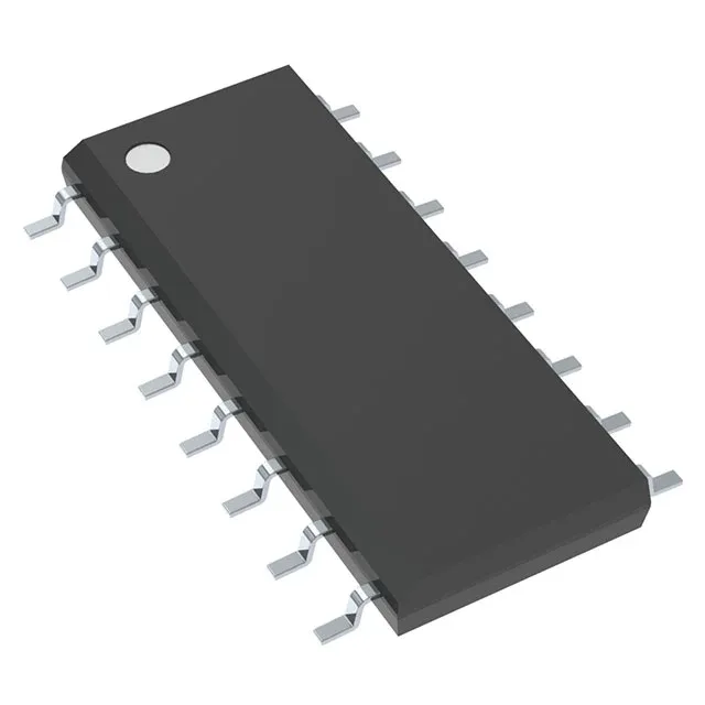
What the 8.1 ns propagation delay means for your timing budget
The 74ACT11032D is a quad 2-input OR gate from Texas Instruments' 74ACT family, built on an advanced CMOS process that combines the speed of bipolar ACT logic with the low power of CMOS. The headline timing number is 8.1 ns max propagation delay at 5 V and 50 pF load. That is the time from when an input crosses the threshold to when the output reaches the valid logic level — and it is the spec that sets the maximum clock rate or data path speed through this gate. In a 5 V system clocked at 50 MHz, the 8.1 ns delay consumes about 40 % of the 20 ns period, so the gate fits comfortably in a single-stage pipeline but leaves limited margin for additional logic in the same cycle. Each of the four gates can sink or source 24 mA at the output, enough to drive a standard TTL load, a small LED, or the input of a downstream CMOS gate without a buffer. The quiescent supply current is just 4 µA max — the part draws almost nothing when the inputs are static, which matters for power-sensitive boards that spend most of their time in a wait state.
Supply voltage and logic thresholds — what fits
The input logic-low threshold is 0.8 V max and the logic-high threshold is 2 V min — these are TTL-compatible levels, meaning the gate interprets a 0.8 V or lower input as a logic 0 and a 2 V or higher input as a logic 1. That matches the output swing of most 5 V CMOS and TTL devices, and it also means a 3.3 V output driving into this gate will be read as a logic 1 as long as it stays above 2 V.