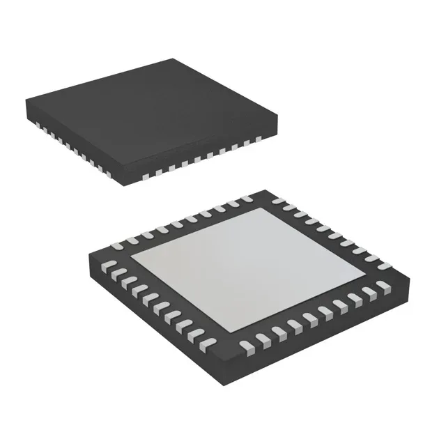
What this clock buffer does on the board
The Texas Instruments LMK00308SQ/NOPB is a 3:9 fanout buffer that also integrates a multiplexer and level translator — one chip handles CML, HCSL, HSTL, LVDS, LVPECL, SSTL, or crystal inputs and fans them out as HCSL, LVCMOS, LVDS, or LVPECL. With a maximum frequency of 3.1 GHz, it sits in high-speed clock trees where you need to distribute a clean reference to multiple endpoints — think FPGA reference clocks, SERDES framing, or ADC/DAC sample clocks. The 40-WQFN package with exposed pad needs a solid thermal via stitch under the paddle if you're running multiple outputs near the frequency ceiling.
3.1 GHz — what that buys you in a clock tree
The 3.1 GHz maximum frequency means this buffer can pass through the fastest common clock standards without reclocking — 10G Ethernet reference clocks, JESD204B SYSREF, or PCIe Gen4/5 reference clocks all fit comfortably. The differential input-to-output path is fully differential (yes/yes), so additive jitter stays low; you are not converting to single-ended and back. At these speeds, the 40-WQFN package's exposed pad is not optional — it is the return path for the output drivers. Plan for a solid ground-plane connection under the part.
Input and output format flexibility
The LMK00308 accepts seven input formats — CML, HCSL, HSTL, LVDS, LVPECL, SSTL, and crystal — and outputs in four: HCSL, LVCMOS, LVDS, LVPECL. That makes it a universal clock-format bridge on a mixed-logic board. If your FPGA bank runs HCSL but the oscillator is LVDS, this part translates in one device. The 3:9 input-to-output ratio gives three selectable input banks feeding nine outputs, which is enough to distribute a master clock to multiple ASICs, FPGAs, and SerDes transceivers without a second fanout stage.
Supply and temperature — industrial range, tight rail
The supply range is 3.15 V to 3.45 V — a tight 3.3 V ±4.5 % window. That is typical for high-speed clock buffers because the output swing and common-mode levels are calibrated to a narrow rail. No AEC-Q grade is listed, so it is not qualified for automotive under-hood use.