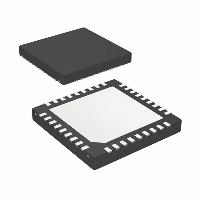
3.1 GHz fanout buffer with universal level translation
The Texas Instruments LMK00306SQ/NOPB is a 3:7 fanout buffer, multiplexer, and translator that accepts CML, HCSL, HSTL, LVDS, LVPECL, SSTL, or crystal inputs and outputs HCSL, LVCMOS, LVDS, or LVPECL. Rated to 3.1 GHz with fully differential I/O, it sits in the clock distribution path of high-speed serial links — PCIe, Ethernet, SerDes, FPGA reference clocks — where signal integrity and jitter budget matter.
Level translation saves board area
Because the LMK00306SQ/NOPB accepts CML, HCSL, HSTL, LVDS, LVPECL, SSTL, and crystal on the input side and outputs HCSL, LVCMOS, LVDS, or LVPECL, it eliminates external level-shifter resistors and AC-coupling capacitors that would otherwise litter the clock tree. For a design mixing, say, an LVDS oscillator feeding an HCSL-input FPGA, this one chip handles the translation and fanout in a single 6x6 mm footprint.
For a BOM line that needs a clock-buffer second source, the closest functional peer is the CDCLVP1204RGTR — 2:4 fanout, LVPECL output only, 2 GHz max, 2.375V supply minimum — but that part lacks the universal input translation and the 3.1 GHz ceiling of the LMK00306. If your design requires the full input flexibility and speed, the LMK00306 is the primary choice; qualify the alternate only if your clock tree can tolerate LVPECL-only output and a lower frequency ceiling.