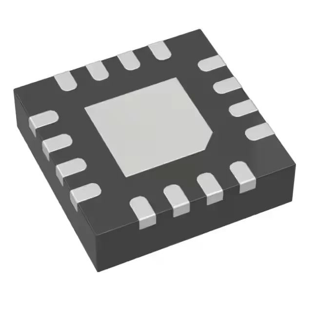
Texas Instruments CDCLVP1102RGTT — Clock & Timing ICs

CDCLVP1102RGTT Fanout Buffer, 2 GHz, 1:2 LVPECL, 16-QFN

MPNCDCLVP1102RGTT
End of Life

Texas Instruments CDCLVP1102RGTT, Fanout Buffer (Distribution), 1:2, LVPECL output, 2 GHz max, 2.375V–3.6V supply, -40°C to 85°C, 16-VFQFN Exposed Pad.

$6.99Ref. price · indicative, final on quote
Packaging16-VFQFN Exposed Pad
StockContact for availability
MOQ1 pcs
  • 100% new & originalTraceable channels only — no refurbs, no pulls, no remarked parts.
  • Date & lot codes on quoteStated per line before you commit; label photos on request.
  • MSL-compliant ESD packingMoisture-sealed bags with indicator cards; reels photo-verified.
  • PayPal buyer protectionPay by T/T, PayPal or Payoneer — card payments covered end to end.

Specifications

CDCLVP1102RGTT Technical Specifications
ParameterValue
TypeFanout Buffer (Distribution)
Mounting typeSurface Mount
Voltage2.375V ~ 3.6V
Frequency2 GHz
Operating temperature-40°C ~ 85°C
InputLVCMOS, LVDS, LVPECL, LVTTL
OutputLVPECL
PackageTape & Reel (TR); Cut Tape (CT)
Case16-VFQFN Exposed Pad
Number of circuits1
Ratio - Input:Output1:2
Differential - Input:OutputYes/Yes

Product details

Clock fanout for high-speed serial links

The Texas Instruments CDCLVP1102RGTT is a 1:2 fanout buffer that takes one clock input and delivers two LVPECL outputs at up to 2 GHz. It accepts LVCMOS, LVDS, LVPECL, or LVTTL levels on the input side, making it a universal glue part between different logic families in a clock tree. The signal path is fully differential from input to output, which preserves edge integrity and common-mode rejection when distributing a reference clock across a PCB. Supply voltage spans 2.375 V to 3.6 V. The industrial temperature range (-40°C to 85°C) suits outdoor telecom.

2 GHz bandwidth — what it means for the clock tree

Because the input accepts multiple standards, you can feed it from a crystal oscillator (LVCMOS) or a previous-stage LVPECL/LVDS source without level-shifting. The output is always LVPECL, so the downstream receivers must be LVPECL-compatible or terminated accordingly.

Sourcing and lifecycle

The CDCLVP1102RGTT is listed as Active in production with ROHS3 compliance.

Frequently asked questions

Is CDCLVP1102RGTT compatible with a 3.3 V supply?

Yes, the supply voltage range of 2.375 V to 3.6 V includes 3.3 V, so it can be powered directly from a 3.3 V rail without an external regulator.

Is CDCLVP1102RGTT obsolete or end-of-life?

No, the CDCLVP1102RGTT is listed as Active in production with no end-of-life notification. It remains suitable for new designs and ongoing production.

What is the output jitter of CDCLVP1102RGTT?

The evidence does not specify an output jitter figure. For jitter performance data, the datasheet should be consulted; the 2 GHz bandwidth and fully differential path are designed to minimise additive jitter in high-speed clock distribution.