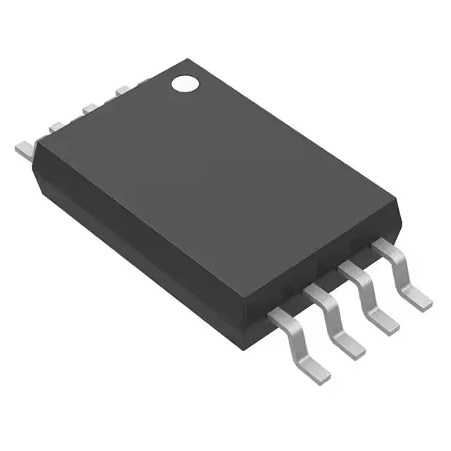
Texas Instruments CDCLVC1102PW — Clock & Timing ICs

CDCLVC1102PW 1:2 LVCMOS Fanout Buffer, 250 MHz, 8-TSSOP

MPNCDCLVC1102PW
End of Life

Texas Instruments CDCLVC1102PW, Fanout Buffer (Distribution), 1:2 LVCMOS, 250 MHz max, 2.3V–3.6V supply, -40°C–85°C, 8-TSSOP package.

$3.57Ref. price · indicative, final on quote
Packaging8-TSSOP (0.173", 4.40mm Width)
StockContact for availability
MOQ1 pcs
  • 100% new & originalTraceable channels only — no refurbs, no pulls, no remarked parts.
  • Date & lot codes on quoteStated per line before you commit; label photos on request.
  • MSL-compliant ESD packingMoisture-sealed bags with indicator cards; reels photo-verified.
  • PayPal buyer protectionPay by T/T, PayPal or Payoneer — card payments covered end to end.

Specifications

CDCLVC1102PW Technical Specifications
ParameterValue
TypeFanout Buffer (Distribution)
Mounting typeSurface Mount
Voltage2.3V ~ 3.6V
Frequency250 MHz
Operating temperature-40°C ~ 85°C
InputLVCMOS
OutputLVCMOS
PackageTube
Case8-TSSOP (0.173\", 4.40mm Width)
Number of circuits1
Ratio - Input:Output1:2
Differential - Input:OutputNo/No

Product details

1:2 LVCMOS fanout buffer — 250 MHz ceiling

The Texas Instruments CDCLVC1102PW is a single-circuit fanout buffer that takes one LVCMOS input and delivers two LVCMOS outputs, rated to 250 MHz. It operates from a 2.3 V to 3.6 V supply, making it a direct fit for 2.5 V and 3.3 V clock trees without an extra regulator. The non-differential input and output (No/No per the differential flag) means simpler board layout — no external termination resistor network needed for the signal path, just standard CMOS drive.

Industrial temperature range — -40°C to 85°C

Rated for -40°C to 85°C operating temperature, this buffer suits outdoor telecom cabinets, factory-floor automation, and motor-drive control boards where the ambient can swing. The 8-TSSOP package (4.40 mm width) is a common footprint for space-constrained layouts, and the surface-mount assembly aligns with standard reflow profiles.

Active lifecycle — no LTB risk

The CDCLVC1102PW carries an Active product status. ROHS3 compliant per the compliance listing, so it passes EU and global material restrictions without an exemption hunt.

Frequently asked questions

Is CDCLVC1102PW RoHS compliant?

Yes, the CDCLVC1102PW is ROHS3 compliant per the lifecycle record, meeting the latest EU RoHS directive without exemptions.

What is the maximum frequency of CDCLVC1102PW?

The CDCLVC1102PW is rated for a maximum frequency of 250 MHz, which defines the upper limit of the clock signal it can cleanly buffer and distribute.

Does CDCLVC1102PW require external termination resistors?

No — because the input and output are both non-differential LVCMOS (single-ended), the CDCLVC1102PW does not require external termination resistors on the signal path. Standard CMOS drive levels apply.