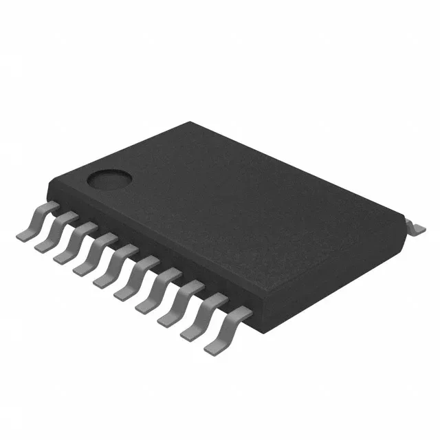
230 MHz PLL clock generator for 1.7 V–1.9 V core rails
The Texas Instruments CDCE937PW is a three-PLL clock synthesizer with integrated VCXO, generating up to seven LVCMOS outputs from a single LVCMOS or crystal input. The 230 MHz maximum output frequency covers common Ethernet, PCIe reference, and FPGA transceiver clock rates, while the 1:7 fanout ratio lets a single PLL feed multiple clock domains on the board. The 1.7 V–1.9 V supply range targets low-voltage core rails found in modern SoCs and FPGAs — not a 3.3 V or 2.5 V peripheral bus.
Supply-voltage check before BOM commitment
The 1.7 V–1.9 V operating range is the first thing to verify against your board's existing power tree. This part will not run from a standard 3.3 V or 2.5 V rail — it needs a dedicated 1.8 V LDO or a switcher set inside that window. If your system already has a clean 1.8 V supply (common for DDR3/4 VTT or certain FPGA core rails), the CDCE937PW drops in without an extra regulator. If not, the added rail cost and board area factor into the BOM decision. The narrow tolerance (1.7 V min, 1.9 V max) also means the supply must be well-regulated; a noisy or loosely-tolerated rail risks PLL jitter or unlock.
Three PLLs, one VCXO — what the architecture buys you
Three independent PLLs with a shared VCXO let you synthesize multiple unrelated frequencies from a single reference crystal, saving a second oscillator. The VCXO path provides fine frequency tuning for applications like spread-spectrum clocking or synchronizing to an external reference. The bypass mode (PLL Yes with Bypass) allows the input clock to feed directly to an output when you need a clean, un-synthesized path — useful during system bring-up or for a jitter-sensitive clock that cannot tolerate PLL noise. All outputs are LVCMOS, so the part interfaces directly with standard digital logic without external level translation.
20-TSSOP package and layout notes
The 20-TSSOP (4.40 mm width) is a common fine-pitch package with 0.65 mm pin pitch — routable on a two-layer board with careful trace spacing. The 1:7 output bank means seven traces leaving the device; group them with matched lengths if skew between clock domains matters. Place the decoupling capacitors (0.1 µF and 1 µF recommended per the reference design) as close to the supply pins as possible, on the same layer, to minimize loop inductance. The exposed thermal pad (if present on the 20-TSSOP variant) should be connected to a ground plane with a via array for heat sinking, though the junction-to-ambient thermal resistance is manageable for this power level.
The base product number CDCE937 indicates a family with multiple frequency and PLL-count variants, so if a future design needs more outputs or a different frequency range, a pin-compatible sibling within the family may be available without a PCB spin.