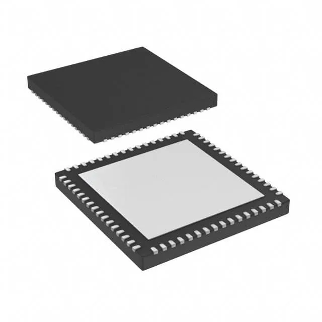
What this part does in a timing tree
The Texas Instruments CDCE72010RGCT is a clock synchronizer, fanout buffer, and jitter cleaner rolled into one device — three functions that typically eat separate board area and skew budgets. It accepts up to three reference inputs (LVCMOS, LVDS, or LVPECL) and fans out to twenty outputs in the same signal formats, with a maximum operating frequency of 1.5 GHz. The single PLL core cleans phase noise on the selected reference before distribution, which is what makes it useful in 10G Ethernet, wireless base station, and instrumentation backplanes where the reference clock arrives noisy from a long cable or a cheap oscillator.
1.5 GHz ceiling — what it buys you
The 1.5 GHz maximum frequency is the spec that separates this part from lower-speed PLLs like the CD74HCT7046AE, which tops out at 38 MHz. At 1.5 GHz the CDCE72010RGCT can directly clock SERDES transceivers, FPGA high-speed transceivers, and ADC/DAC sample clocks without an external frequency multiplier. The 3:20 input-to-output ratio means a single device can replace a clock mux plus a fanout buffer plus a jitter attenuator — three ICs and their associated PCB trace stubs.
ROHS3 compliant.