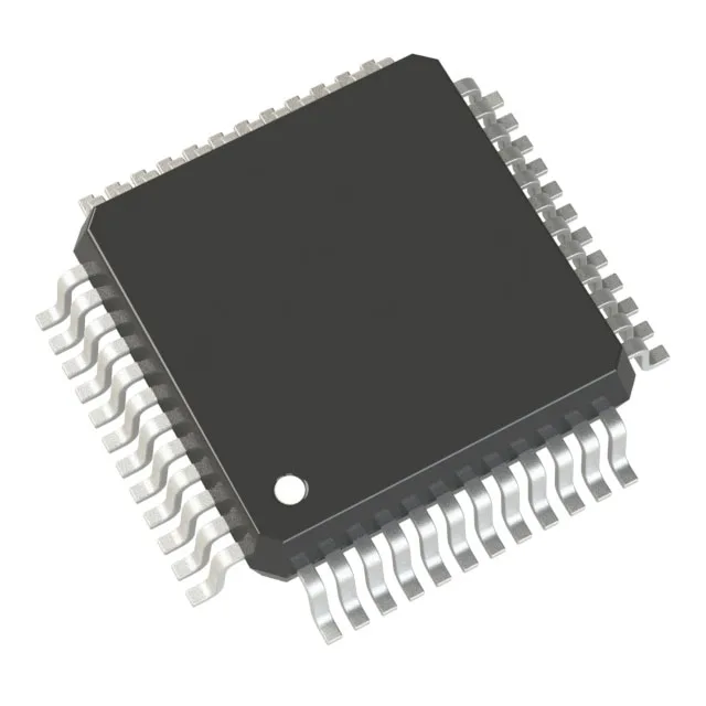
48-LQFP package and board integration
The STM32L031C6T7: The pad is not an electrical connection; it is the thermal path to the ground plane. A 0.3 mm via under the pad drops the junction-to-board thermal resistance by roughly 15 °C/W compared to relying on the leadframe alone.
Memory partition and firmware-fit check
32 KB flash (32K x 8) with 8 KB SRAM and 1 KB embedded EEPROM. The EEPROM is mapped into a separate address space — no wear-leveling needed for infrequent parameter storage, but the 100k-cycle endurance per byte is shared across the whole 1 KB block. A typical sensor-node firmware with FreeRTOS kernel (~6 KB), HAL drivers (~8 KB), and application code leaves roughly 18 KB free. The 8 KB SRAM holds the stack, heap, and a single 2 KB DMA buffer; budget the linker script accordingly.
The brown-out reset threshold is programmable in 100 mV steps from 1.8 V to 2.7 V — set it at 2.0 V for a two-alkaline design to catch the cell before the SRAM contents corrupt. At 32 MHz the typical run current is 8.3 mA from flash; in Stop mode with the RTC running it drops to 1.2 µA.
-40°C to 105°C ambient (TA) — the T7 suffix denotes this industrial temperature range. The internal oscillator is trimmed at 25°C and drifts ±1% across the full temperature band; for a UART baud rate above 115200, switch to the external HSE crystal. The 12-bit ADC offset error doubles below 0°C — budget a one-point calibration at the cold end if the application reads sub-zero temperatures.
Peripherals and connectivity
38 GPIOs in the 48-LQFP — 10 pins are consumed by VDD/VSS, the oscillator, and the NRST pin. The remaining 38 include two I²C (one with SMBus timeout), two SPI (one with 16-bit FIFO), and three USARTs (one with LIN and IrDA support). The 10-channel 12-bit ADC samples at 1.14 Msps max — enough for three-phase current sensing at 10 kHz per phase plus a thermistor input. DMA is available on all major peripherals; the PWM timer has six independent channels with dead-time insertion.