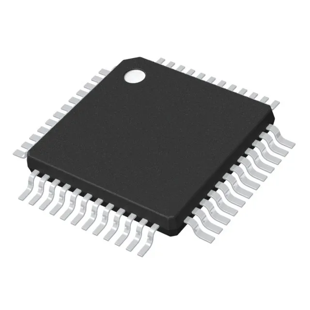
Core and memory budget for the BOM line
The STM32G070CBT6 runs an ARM Cortex-M0+ core at 64 MHz — the entry-level 32-bit architecture that displaces 8/16-bit parts in cost-sensitive designs where the 32-bit data path and 4 GB address space matter more than raw DMIPS. 128 KB of on-chip flash and 36 KB of SRAM (organized as 36K x 8) give the firmware stack room for a real-time kernel, a modest protocol stack, and a sensor-fusion loop without external memory. The 48-LQFP package (7x7 mm body) exposes 43 I/O pins — nearly every package pin is a GPIO or alternate-function pin, which is unusual for a 48-pin MCU and means fewer wasted pins in a tight layout.
Peripheral set and deployment context
On-chip peripherals include DMA, I²S, POR, PWM, and WDT — enough to run a motor-control loop with sensor feedback or a multi-drop sensor network without external timers or watchdog ICs. The 17-channel 12-bit ADC captures analog inputs from thermistors, current shunts, or potentiometers on a single scan sequence. The -40 to 85°C temperature grade qualifies the part for factory-floor enclosures, HVAC controllers, and outdoor telecom cabinets that see seasonal temperature swings. Supply range of 2.0 to 3.6 V means the MCU runs from a single 3.3 V rail or two alkaline cells in series — no extra regulator needed for battery-powered edge nodes.
That means it is safe to qualify into a new design today without planning a mid-life migration.