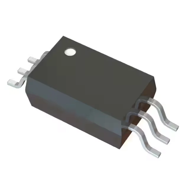
10 Mbps isolation barrier for noisy industrial links
The PS9317L-V-AX is a single-channel optocoupler rated for 10 Mbps data throughput with 5000 Vrms galvanic isolation — enough to break ground loops between a motor-drive power stage and the controller-side logic while keeping a 10 Mbps SPI or UART link intact. The open-collector output sinks 25 mA per channel, which drives the input of a downstream PLC or MCU directly without an external buffer transistor. Common-mode transient immunity is specified at 15 kV/µs minimum — a figure that matters when the optocoupler straddles a switching node where the ground plane jumps several hundred volts in tens of nanoseconds; below this threshold the output glitches and the link drops bits.
Timing budget and edge symmetry
Propagation delay is 75 ns max for both low-to-high and high-to-low transitions — the symmetric spec means the pulse-width distortion stays within the same window, so a 10 Mbps NRZ signal does not accumulate duty-cycle error across the barrier. Rise time is 20 ns typical, fall time 5 ns typical — the asymmetric edges shift the output duty cycle by about 15 ns at 10 Mbps; the downstream receiver should have a Schmitt-trigger input or a 10 % timing margin to avoid missing the first bit after a long idle. Operating temperature spans -40 to 85 °C, which covers the industrial enclosure environment but not extended under-hood or engine-bay applications — for 105 °C or higher, look at the -VY or extended-grade variants in the same package.
Package, footprint, and supply rails
Housed in a 6-SOIC package with 6.80 mm body width (0.268 inch) and an SDIP (staggered dual-inline) lead form — the footprint matches a standard SOIC-6 land pattern, but the SDIP lead pitch is 1.27 mm staggered, so verify the solder-paste stencil aperture against the package drawing if using a single-row pad layout. The input LED is rated for 20 mA max forward current with a typical forward voltage of 1.56 V at that current — a 180 Ω series resistor from a 5 V rail sets the drive current at roughly 19 mA, staying inside the abs-max limit.