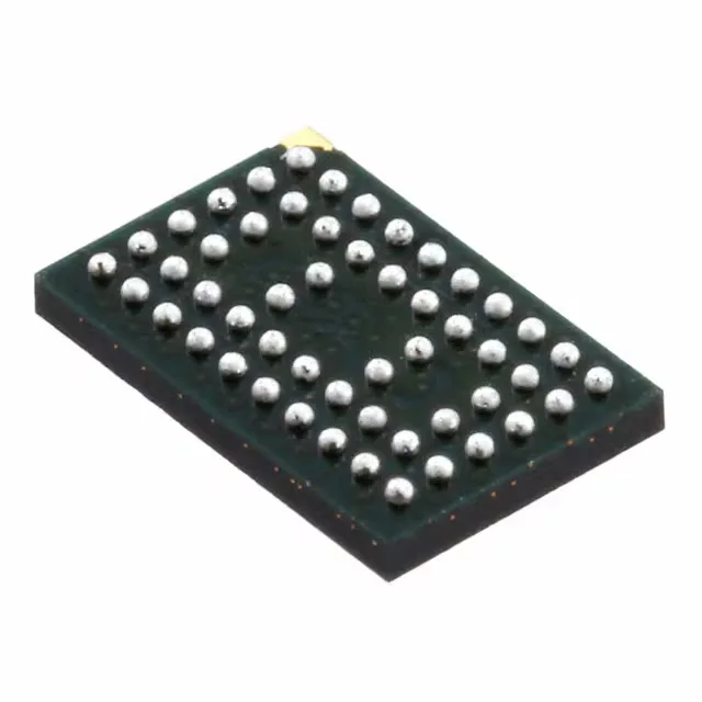
Clock distribution for DDR2 memory buses
The CSPUA877ABVG is a 1:10 SDRAM clock driver purpose-built for DDR2 memory interfaces, distributing a single differential clock input to ten low-skew outputs at up to 410 MHz. Both input and output paths are differential (Yes/Yes), preserving signal integrity over the multi-drop DDR2 bus where common-mode noise rejection matters. The 1.7 V to 1.9 V supply range aligns with the DDR2 memory controller and DIMM voltage rails, so no external level translation is needed between the driver and the DRAM clock inputs.
Housed in a 52-VFBGA (4.5x7.0 mm CABGA), the fine-pitch BGA footprint demands a controlled-impedance PCB layout — the differential clock traces must be length-matched to within the driver's output-to-output skew budget to keep setup/hold margins on the DRAM side.