Supply range and page organization
The AT45DB021E-SSHN-B: Supply range is 1.65 V to 3.6 V. Page size is 264 bytes. Word write is 8 µs; page write is 3 ms.
Active lifecycle, no LTB risk
No last-time-buy notice or end-of-life announcement exists.
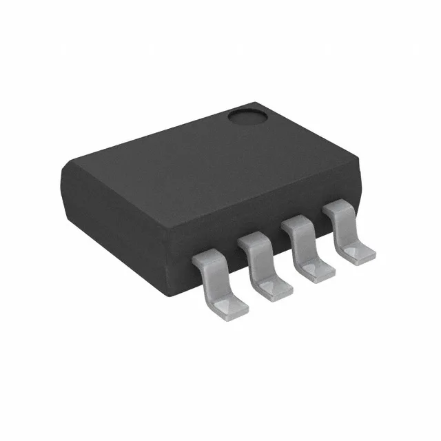
Adesto / Dialog AT45DB021E-SSHN-B, 2Mbit SPI DataFlash, 70 MHz clock, 1.65 V–3.6 V supply, 264 B × 1024 pages, 8-SOIC package, tube, -40 °C to 85 °C.
| Parameter / Attribute | Specification / Value |
|---|---|
| Memory type | Non-Volatile |
| Mounting | Surface Mount |
| Supply voltage | 1.65V ~ 3.6V |
| Clock frequency | 70 MHz |
| Memory interface | SPI |
| Operating temperature | -40°C ~ 85°C (TC) |
| Package | Tube |
| Technology | FLASH |
| Memory size | 2Mbit |
| Memory format | FLASH |
| Case | 8-SOIC (0.154\", 3.90mm Width) |
| Memory organization | 264 Bytes x 1024 pages |
| Write cycle time - word, page | 8µs, 3ms |
Factory lead times blocking production? We lock verified brand-new original stock in Shenzhen within 2 hours.
Direct access to Shenzhen floor inventory, franchised allocation buffers, and factory bonded stock to resolve line-down shutdowns.
Standard factory-sealed packaging compliant with EIA-481 standards for automated high-speed SMT pick-and-place lines.
High-resolution photos of original reel labels, 2D DataMatrix, and pin coplanarity sent via WhatsApp/Telegram before you release wire payment.
The AT45DB021E-SSHN-B: Supply range is 1.65 V to 3.6 V. Page size is 264 bytes. Word write is 8 µs; page write is 3 ms.
No last-time-buy notice or end-of-life announcement exists.
This part is sourced through independent distribution. Submit an RFQ for current availability and pricing; lead time and price are confirmed at quote time.
The page write time is 3 ms; the word write time is 8 µs.
Yes. The -B (tube) and -T (tape-and-reel) variants share the same die, same 8-SOIC package, same 70 MHz SPI interface, same 1.65 V–3.6 V supply, and same 264-byte page organization. The only difference is the delivery medium.
The AT45DB021E series is the successor to the AT45DB021D and maintains the same 8-pin SOIC footprint and SPI pinout. Verify the exact supply voltage and timing parameters against your design, but the mechanical and interface compatibility is preserved across the E and D generations.
The listed interface is standard SPI. The DataFlash family does not include quad-SPI support on this part; it uses a single SPI bus with dedicated chip-select, clock, data-in, and data-out lines.