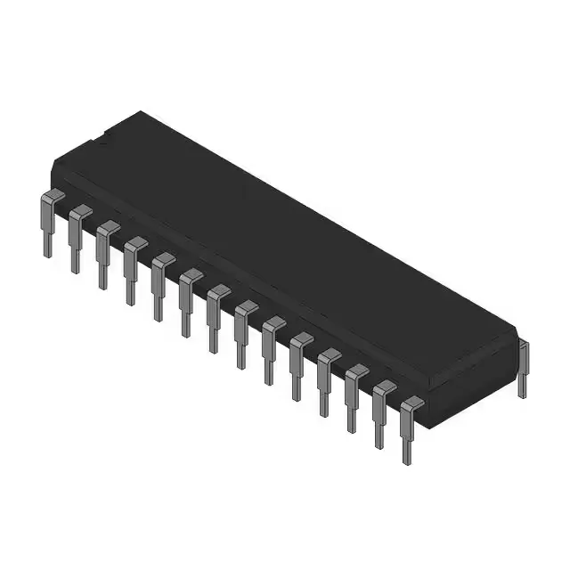
256Kbit asynchronous SRAM in hermetic ceramic DIP
The Renesas Electronics 71256L55TDB is a 256 Kbit parallel asynchronous SRAM organized as 32K x 8 bits, with a 55 ns access time. The hermetic ceramic package and wide temperature grade target deployment in avionics, missile guidance, satellite subsystems, and downhole instrumentation where plastic-packaged commercial or industrial SRAMs cannot survive thermal cycling or outgassing requirements.
55 ns access time and asynchronous interface
The 55 ns access time (tAA) governs the read-cycle timing: the address-to-data-valid delay. For a CPU or DSP with a 12.5 MHz bus clock (80 ns cycle), this SRAM fits without wait states. The write cycle time, word/page, is also 55 ns, so the bus master must hold the write strobe and data valid for at least that window. As an asynchronous device, the 71256L55TDB requires no clock input — the chip-enable (CE) and output-enable (OE) pins gate the data bus directly. This simplifies board routing and timing closure in point-to-point or low-density memory maps compared to synchronous SRAMs that need a free-running clock and PLL.
Package, temperature grade, and board integration
The ceramic body is hermetically sealed; no moisture sensitivity level (MSL) rating applies, so no bake-out is needed before reflow or hand-soldering. Decoupling should follow the usual 0.1 µF ceramic per supply pin, placed within 0.25 inches of the VCC and GND pins, with a bulk 10 µF tantalum near the device on the 5V rail.