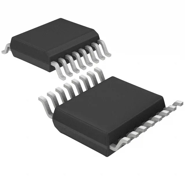
What this 1:8 LVCMOS fanout buffer does on the board
The Renesas 5PB1108PGGI is a single-channel fanout buffer that takes one LVCMOS clock input and distributes it to eight LVCMOS outputs. It handles clock frequencies up to 200 MHz and runs from a supply rail between 1.71 V and 3.465 V, so it can sit on a 1.8 V or 3.3 V logic plane without a separate level translator.
That matters when the fanout drives a load expecting 3.3 V logic levels. The input is also LVCMOS, so there is no differential receiver; you cannot feed it a LVPECL or LVDS signal without an external converter. The non-differential I/O (No/No per the spec) is a hard constraint for designs using AC-coupled or CML clock sources.
It is not AEC-Q100 qualified, so it is not the pick for engine-control or chassis-domain clock trees.
That removes the last-time-buy risk for a production BOM line.