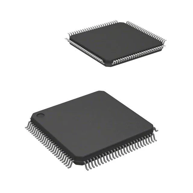
NXP Semiconductors MK10DN512VLL10 — Analog & Data Acquisition

NXP MK10DN512VLL10 Kinetis K10 MCU, ARM Cortex-M4 100MHz

MPNMK10DN512VLL10
End of Life

NXP Kinetis K10 MK10DN512VLL10, 32-bit ARM Cortex-M4 MCU, 100MHz, 512KB Flash, 128KB RAM, 70 I/O, 100-LQFP, -40 to 105°C.

$15.88Ref. price · indicative, final on quote
Packaging100-LQFP
StockContact for availability
MOQ1 pcs
  • 100% new & originalTraceable channels only — no refurbs, no pulls, no remarked parts.
  • Date & lot codes on quoteStated per line before you commit; label photos on request.
  • MSL-compliant ESD packingMoisture-sealed bags with indicator cards; reels photo-verified.
  • PayPal buyer protectionPay by T/T, PayPal or Payoneer — card payments covered end to end.

Specifications

MK10DN512VLL10 Technical Specifications
ParameterValue
SeriesKinetis K10
Mounting typeSurface Mount
Oscillator typeInternal
Program memory typeFLASH
Voltage - supply (Vcc (Vdd))1.71V ~ 3.6V
Operating temperature-40°C ~ 105°C (TA)
Speed100MHz
PackageTray
RAM size128K x 8
Core size32-Bit Single-Core
PeripheralsDMA, I²S, LVD, POR, PWM, WDT
ConnectivityCANbus, EBI/EMI, I²C, IrDA, SD, SPI, UART/USART
Number of i (O)70
Core processorARM® Cortex®-M4
Case100-LQFP
Data convertersA/D 37x16b; D/A 1x12b
Program memory size512KB (512K x 8)

Product details

Kinetis K10 at 100 MHz — what the core delivers

The NXP MK10DN512VLL10 is a 32-bit ARM Cortex-M4 microcontroller from the Kinetis K10 series, clocked at 100 MHz. It carries 512 KB of Flash program memory and 128 KB of SRAM, with 70 general-purpose I/O lines brought out to a 100-LQFP (14x14 mm) package. The part is rated for the industrial temperature range of -40°C to 105°C.

Peripheral set and analog integration

On-chip peripherals include DMA, I²S, LVD, POR, PWM, and WDT, plus connectivity for CANbus, EBI/EMI, I²C, IrDA, SD, SPI, and UART/USART. The data converter block integrates a 37-channel 16-bit ADC and a single 12-bit DAC, which can reduce external analog front-end components in sensor interface and closed-loop control designs. An internal oscillator is available, though an external crystal can be used for tighter timing budgets.

Package and footprint considerations

The 100-LQFP package with a 14x14 mm body is a standard footprint. The supplier device package code is 100-LQFP (14x14).

Lifecycle and sourcing posture

It is ROHS3 compliant. For BOM planning, this part is available through independent distribution and is quoted to order against an RFQ.

Frequently asked questions

Can the MK10DN512VLL10 replace the MK10DN512VLK10?

The MK10DN512VLK10 is a sibling in the same Kinetis K10 family. The key difference is the package: the VLL10 suffix indicates a 100-LQFP, while the VLK10 uses a different package variant. Pin compatibility depends on the specific package footprint — verify the package/case code against your PCB layout before substituting. Both share the same core, memory, and peripheral set.

Is the MK10DN512VLL10 compatible with 3.3V logic?

Yes, the MK10DN512VLL10 operates from 1.71 V to 3.6 V, so it runs directly on a 3.3 V supply rail. The I/O are 5 V tolerant on most pins, allowing direct connection to 3.3 V and many 5 V logic families without external level shifters.

What is the core speed of the MK10DN512VLL10?

The ARM Cortex-M4 core runs at 100 MHz. At this clock rate, the flash memory requires zero wait states for most accesses; the internal bus matrix supports concurrent DMA and CPU transactions without stalling.