Single-core Cortex-A9 at 800 MHz — where the speed ceiling lands
The MCIMX6S7CVM08AC runs a single ARM Cortex-A9 core at 800 MHz. That clock rate, combined with the NEON SIMD coprocessor, sets the throughput boundary for real-time control loops, HMI rendering, and protocol stack processing — the part can sustain a 100 ms control cycle with margin for a modest UI refresh, but a 1 ms servo loop would push the core to its limit without offloading to the NEON or a dedicated peripheral. This is the solo-core member of the i.MX6S series — no second Cortex-A9 or Cortex-M4 companion core. For a design that needs deterministic low-latency response alongside a rich OS, the single core means the application must partition the interrupt load and avoid priority inversion in the scheduler.
Memory controller flexibility — LPDDR2, LVDDR3, DDR3
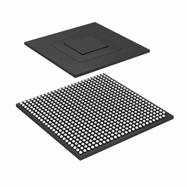
The integrated RAM controller supports LPDDR2, LVDDR3, and DDR3. That lets the BOM engineer choose a memory type based on cost per bit, board layer count, and power budget — LPDDR2 draws less standby current for a battery-backed design, while DDR3 offers the lowest per-MB cost for a mains-powered panel with a 512 MB or 1 GB footprint. The 624-MAPBGA (21x21 mm) package with 0.8 mm ball pitch requires a 4-layer PCB minimum for fan-out of the DDR signals and the Ethernet differential pairs. The 21 mm body fits standard industrial form factors but the via pattern under the BGA must be planned for the DDR3 fly-by topology.
Peripheral set for an industrial gateway or HMI
Four USB 2.0 ports with integrated PHY mean no external USB transceiver is needed for host or device roles — enough for a touchscreen, a Wi-Fi dongle, a USB camera, and a service port. The single Gigabit Ethernet MAC (10/100/1000 Mbps) connects to an external PHY for the plant network uplink or a fieldbus gateway. The display controller drives a direct LCD panel without an external display bridge — the LCD controller and keypad interface handle a basic HMI. For a 7-inch WVGA panel at 60 Hz, the memory bandwidth from the DDR controller is sufficient without stalling the CPU. Additional interfaces include CAN, I2C, I2S, MMC/SD/SDIO, SAI, SPI, SSI, and UART — covering industrial fieldbus (CAN), audio codec (I2S/SAI), and storage (SDIO for eMMC or SD card). The I2C and SPI buses handle sensor and ADC communication without external GPIO expanders.
Security and tamper resistance for field-deployed equipment
The security subsystem includes ARM TrustZone, boot security, cryptography acceleration, a secure fuse box, secure JTAG, secure memory, a secure RTC, and tamper detection. For a device that must resist firmware extraction or field tampering — such as a payment terminal, a metering gateway, or a medical pump — these features allow a chain of trust from boot to application without an external secure element.