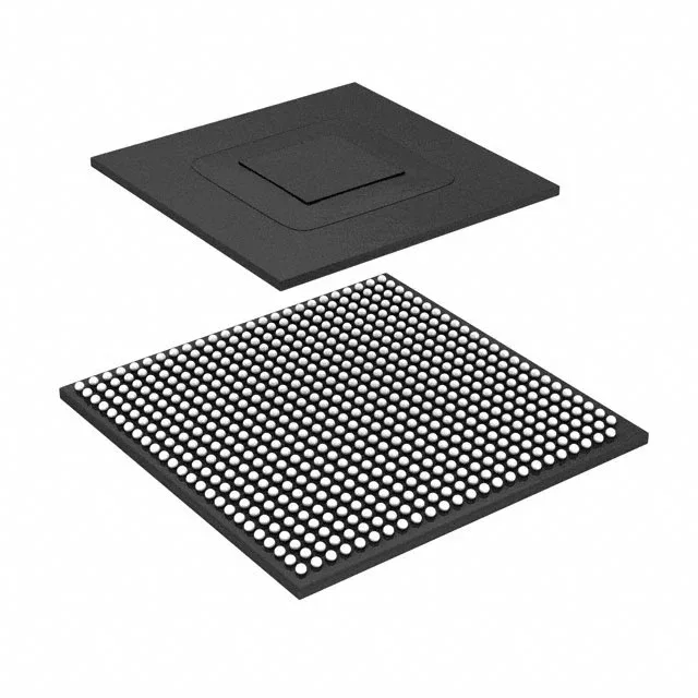
Single-core Cortex-A9 at 800 MHz — industrial HMI and control sweet spot
The MCIMX6S7CVM08ACR is the single-core member of NXP's i.MX6S series, built around an ARM Cortex-A9 core clocked at 800 MHz. This is the cost-optimized entry point for the i.MX6 family — it shares the same peripheral set and package footprint as the dual- and quad-core variants, so a single PCB layout serves the whole range. The 800 MHz ceiling is set by the core speed, not the memory bus — the Cortex-A9 pipeline sustains 2.5 DMIPS/MHz, delivering roughly 2000 DMIPS. For an HMI panel refreshing a 1024x600 display at 60 fps with a touch controller and Ethernet polling, this leaves headroom for the application stack and RTOS overhead.
Memory flexibility and peripheral integration
The memory controller supports LPDDR2, LVDDR3, and DDR3 — three voltage domains on one interface. This lets a design reuse an existing DDR3 layout from a previous i.MX6 project or switch to LPDDR2 for lower standby power in battery-backed equipment. The 32-bit bus width delivers roughly 4.2 GB/s peak bandwidth at 533 MHz, enough for a 1080p display buffer and Ethernet DMA without stalling the core. Four USB 2.0 ports with integrated PHY eliminate external ULPI transceivers — each PHY saves about 15 mm² of board area and $0.30 in BOM cost. The single Gigabit Ethernet MAC with RGMII interface connects to an external PHY; the 10/100/1000 Mbps rate auto-negotiates, so the same magnetics work across all three speeds. The I/O voltage bank is configurable per group at 1.8V, 2.5V, 2.8V, or 3.3V — this matters when interfacing to a 1.8V DDR3 memory on one bank and a 3.3V NOR flash on another. The voltage domains are isolated, so a short on one bank does not pull down the others. Security features include ARM TrustZone, secure boot with OTP fuses, a cryptographic accelerator, and tamper detection inputs. For a connected industrial controller that must meet IEC 62443-4-2 SL2, these blocks handle the secure boot chain and session key exchange without a separate TPM chip.
Industrial temperature range and package integration
The 105°C upper limit is the junction temperature; the 21x21 mm 624-MAPBGA package has a theta-JA of roughly 18°C/W with a 2 oz copper plane, so a 1.5 W typical load keeps the junction below 100°C at 70°C ambient. The 624-ball BGA uses a 0.8 mm pitch — standard for this pin count. Four-layer PCB fan-out is feasible with 0.2 mm trace/space; six layers give cleaner routing for the DDR3 fly-by topology and the Ethernet RGMII traces. The exposed paddle on the bottom of the package must be soldered to a thermal via array under the BGA — without it, the junction temperature rises 5-8°C under full load.
Active lifecycle — sourcing posture for production
The tape-and-reel packaging (TR) is standard for this BGA; cut-tape (CT) is available for prototyping or low-volume builds.