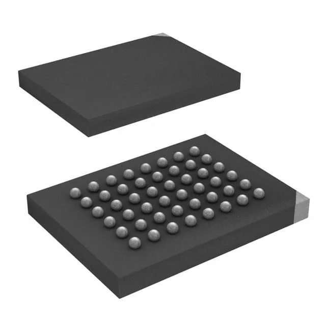
Active parallel NOR flash for legacy memory-mapped buses
The SST38VF6402B-70I/CD is a 64Mbit parallel NOR flash organized 4M x 16 with a 70 ns access time. Active lifecycle status means no end-of-life watch for current BOM positions — no lifetime-buy trigger required.
70 ns access time and bus timing margin
At 70 ns access time the part meets the read-cycle timing of most 16-bit MCUs and DSPs running below 30 MHz without wait states. Memory interface is parallel — not SPI — so it directly maps into the processor's external bus, preserving code-execute performance without serial overhead. Write cycle time per word or page is 10 µs, typical for NOR flash; bulk erase is slower and datasheet-typical.
Package and PCB layout: 48-TFBGA fan-out
Housed in a 48-TFBGA measuring 6x8 mm — the 0.50 mm ball pitch requires a 4-layer PCB with via-in-pad or microvia fan-out; a 2-layer board does not break out the inner rows.
Temperature grade and application environment
Supply voltage range is 2.7V to 3.6V, compatible with 3.3V logic families without a level shifter on the memory bus.