Microchip Technology DSPIC33EP256MC202-I/MM — Interface & Transceivers

Microchip DSPIC33EP256MC202-I/MM dsPIC33EP MCU, 70 MIPs

MPNDSPIC33EP256MC202-I/MM
End of Life

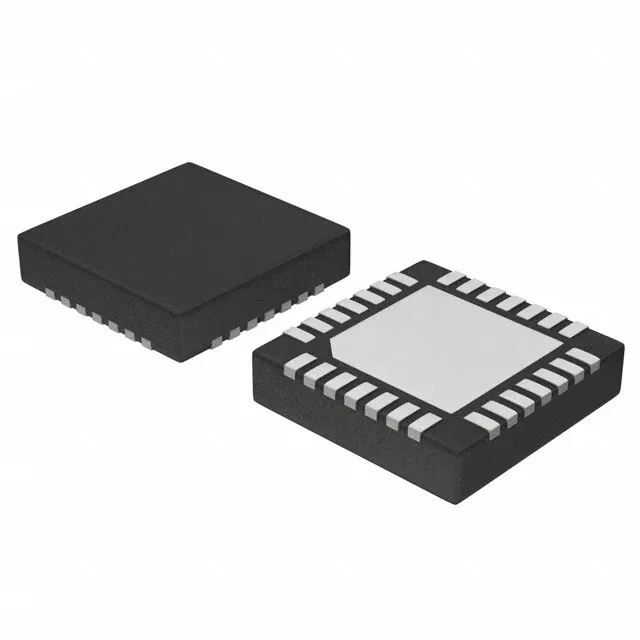
Microchip dsPIC33EP series, DSPIC33EP256MC202-I/MM, 16-bit DSC, 70 MIPs, 256KB Flash, 16K x 16 RAM, 21 I/O, Motor Control PWM, DMA, 3V-3.6V, -40°C to 85°C, 28-QFN-S (6x6).

$4.21Ref. price · indicative, final on quote
Packaging28-VQFN Exposed Pad
RoHSROHS3 Compliant
SeriesdsPIC™ 33EP
Independent supplier — new & surplus stockAuthenticity-screened · ESD-safe packingListing updated Jul 2026

Specifications

DSPIC33EP256MC202-I/MM specifications
ParameterValue
SeriesdsPIC™ 33EP
MountingSurface Mount
Oscillator typeInternal
Program memory typeFLASH
Voltage - supply (Vcc (Vdd))3V ~ 3.6V
Operating temperature-40°C ~ 85°C (TA)
Speed70 MIPs
PackageTube
RAM size16K x 16
Core size16-Bit
PeripheralsBrown-out Detect/Reset, DMA, Motor Control PWM, POR, PWM, WDT
ConnectivityI²C, IrDA, LINbus, QEI, SPI, UART/USART
Number of i (O)21
Core processordsPIC
Case28-VQFN Exposed Pad
Data convertersA/D 6x10b/12b
Program memory size256KB (85.5K x 24)

Product details

70 MIPs in a 28-QFN — what that buys you

The Microchip DSPIC33EP256MC202-I/MM is a 16-bit digital signal controller from the dsPIC33EP family, packing 70 MIPs of deterministic execution into a 28-QFN-S package. The 21 I/O lines, Motor Control PWM peripheral, and DMA controller let you offload PWM updates and ADC reads from the core — the CPU stays free for the control law while the DMA handles the data movement.

Peripheral set and deployment context

The peripheral list includes a dedicated Motor Control PWM module, a quadrature encoder interface (QEI), and a 6-channel A/D converter with 10-bit or 12-bit resolution. These map directly to the signal chain of a three-phase BLDC or PMSM drive: the QEI reads rotor position, the PWM generates the switching pattern, and the ADC samples phase currents — all coordinated by the DMA without jitter from interrupt latency. Supply voltage is 3V to 3.6V, which aligns with a 3.3V rail common in mixed-signal designs.

For BOM planning, this is a single-source Microchip part without a direct pin-compatible second source from another vendor. The PIC24FJ256GA106-I/MR is a 16-bit PIC24 with the same Flash density but runs at 32 MHz and lacks the DSP engine and Motor Control PWM, so it is not a functional substitute for a dsPIC33EP design. If the application relies on the 70 MIPs and the PWM/DMA peripherals, this is the part the BOM stays with.

Frequently asked questions

Can DSPIC33EP256MC202-I/MM replace DSPIC33EP256MC202-I/SO?

The -I/SO suffix indicates an SOIC-28 package; the -I/MM is a 28-QFN-S (6x6 mm) package. They are electrically identical in core and peripherals, but the footprint differs — the QFN has an exposed pad for thermal dissipation and a smaller land pattern. A board designed for the SOIC cannot take the QFN without a layout change, and vice versa. The operating temperature range and supply voltage are the same.