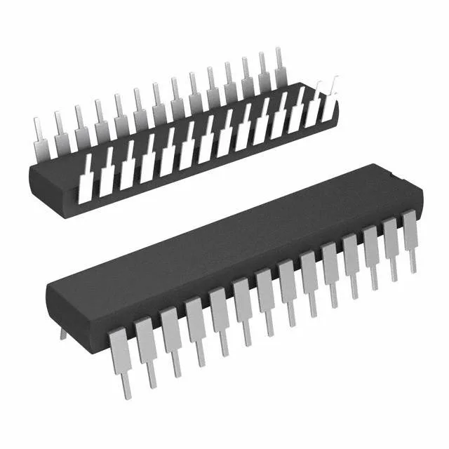
Microchip Technology DSPIC33EP128GP502-I/SP — Discrete Semiconductors

Microchip DSPIC33EP128GP502-I/SP 16-bit MCU, 70 MIPs

MPNDSPIC33EP128GP502-I/SP
End of Life

Microchip dsPIC™ 33EP series, DSPIC33EP128GP502-I/SP, 16-bit dsPIC core, 70 MIPs, 128KB (43K x 24) FLASH, 8K x 16 RAM, CANbus/I²C/SPI/UART, 21 I/O, 6x10b/12b ADC, 3V-3.6V, -40°C to 85°C, 28-SPDIP through-hole.

$4.51Ref. price · indicative, final on quote
Packaging28-DIP (0.300", 7.62mm)
RoHSROHS3 Compliant
SeriesdsPIC™ 33EP
Independent supplier — new & surplus stockAuthenticity-screened · ESD-safe packingListing updated Aug 2026

Specifications

DSPIC33EP128GP502-I/SP specifications
ParameterValue
SeriesdsPIC™ 33EP
MountingThrough Hole
Oscillator typeInternal
Program memory typeFLASH
Voltage - supply (Vcc (Vdd))3V ~ 3.6V
Operating temperature-40°C ~ 85°C (TA)
Speed70 MIPs
PackageTube
RAM size8K x 16
Core size16-Bit
PeripheralsBrown-out Detect/Reset, DMA, POR, PWM, WDT
ConnectivityCANbus, I²C, IrDA, LINbus, SPI, UART/USART
Number of i (O)21
Core processordsPIC
Case28-DIP (0.300\", 7.62mm)
Data convertersA/D 6x10b/12b
Program memory size128KB (43K x 24)

Product details

Memory and throughput for closed-loop control

The 70 MIPs execution rate is the key spec for a control-loop designer: at 70 million instructions per second, a 10 kHz current-control loop has 7000 instruction cycles per iteration, enough for a PID with feedforward and a sensor filter. The 128 KB Flash (43K x 24) holds the firmware and a lookup table for motor profiles or sensor linearisation, while the 8K x 16 SRAM buffers ADC samples and state variables without spilling to external memory. The six-channel 10-bit/12-bit ADC (A/D 6x10b/12b) samples synchronously with the PWM timers, so the controller reads phase currents at the switching edge without software jitter. The DMA peripheral moves ADC results directly to RAM without CPU intervention, preserving MIPs for the control algorithm.

28-SPDIP: through-hole fit and board assembly

The 28-pin SPDIP (0.300-inch row spacing, 7.62 mm body width) is a through-hole package that suits hand-assembly, rework, or low-volume wave-solder production. The 21 general-purpose I/O lines are enough for a sensor interface with a few discrete outputs; the remaining pins are dedicated to the oscillator, supply, and programming/debugging (ICSP). The 3V to 3.6V supply rail is common to 3.3V systems; a single 3.3V regulator with a 100 nF decoupling cap per supply pin is the standard bypass recommendation.

Frequently asked questions

What voltage does DSPIC33EP128GP502-I/SP operate at?

The supply voltage range is 3V to 3.6V. This 3.3V nominal rail is common in industrial and automotive systems; a single 3.3V regulator with proper decoupling per supply pin is sufficient.

What is DSPIC33EP128GP502-I/SP's listed speed?

The core runs at 70 MIPs. That is the instruction throughput ceiling for the dsPIC33EP family, and it determines the maximum control-loop bandwidth and sensor-fusion update rate the processor can sustain without external memory wait states.

Is DSPIC33EP128GP502-I/SP equivalent to other dsPIC33EP parts?

Within the dsPIC33EP family, the 128KB Flash and 8K x 16 RAM configuration with 28-SPDIP package is a specific density and footprint tier. Higher-density siblings (e.g., 256KB or 512KB Flash) are available in larger pin-count packages, but they are not pin-compatible with the 28-SPDIP. The 21 I/O and 6-channel ADC count are fixed by the 28-pin package.