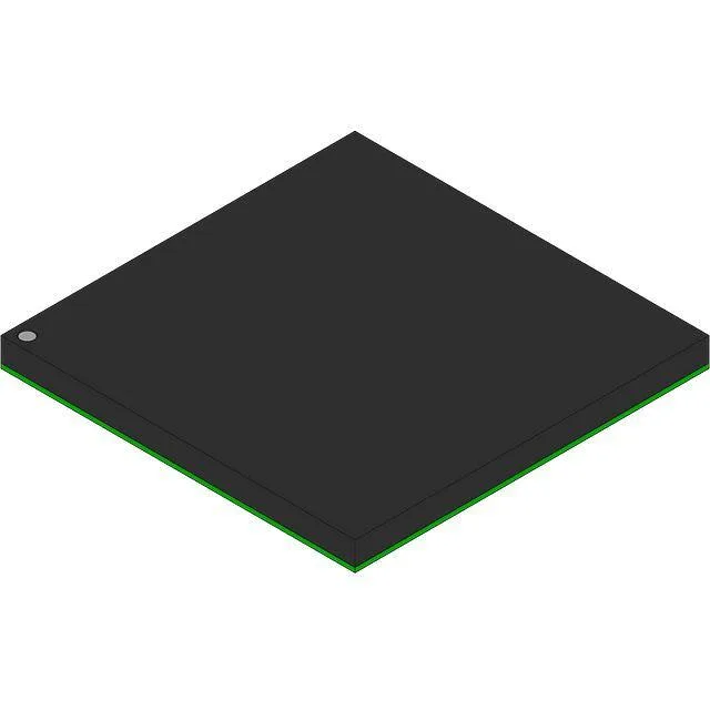
Lattice Semiconductor OR4E04-3BM680C — FPGA / CPLD & Programmable Logic
Technical Documents PDF / CAD
RoHS Compliant · Lead-Free EIA-481 Standard
Lattice Semiconductor / FPGA / CPLD & Programmable Logic

Lattice OR4E04-3BM680C ORCA4 FPGA, 10368 LEs, 466 I/O

MPN OR4E04-3BM680C
Active Spot Stock · 24-48h Dispatch 100% Original Sealed

Lattice Semiconductor ORCA™4 FPGA, OR4E04-3BM680C, 10368 logic elements, 466 I/O, 643000 gates, 113664 bits block RAM, 1.425 V core, 0°C to 70°C, Bulk.

Factory Allocation · Direct Sourcing
MOQ: 1 pcs
Logistics: DHL / FedEx DAP (Global Express · 3-7d) Russia & CIS DDP (Door-to-Door Cleared)
Dispatch: Shenzhen / HK
Wholesale Ref. Price (USD)
Target Price / Quote (2h Fast Turnaround)
Formal B2B Quotation in 2h
Volume pricing applies from 1,000 pcs upward, and is confirmed per order against the quantity and the shipment date. Inquire for Target Qty →
Working on a production BOM or have a target unit price? Submit Target Price
[SPEC] Essential Parameters Snapshot Full Specifications (11)
Supply Voltage 1.425

Full Technical Specifications

11 Parameters
OR4E04-3BM680C specifications
Parameter / AttributeSpecification / Value
SeriesORCA™4
MountingSurface Mount
Operating temperature high0°C to 70°C(TA)
Package_typeBulk
Number of i (O)466
Total ram bits113664
StatusActive
Number of gates643000
Supply voltage1.425
Number of labs (Clbs)1296
Number of logic elements (Cells)10368
[DESK] Shenzhen Spot Allocation · 2h Response

Need Immediate Spot Stock or Shortage Allocation for OR4E04-3BM680C?

Factory lead times blocking production? We lock verified brand-new original stock in Shenzhen within 2 hours.

Quote SLA 2 Hours
[01] Emergency Shortage 24-48h Shenzhen Dispatch

Direct access to Shenzhen floor inventory, franchised allocation buffers, and factory bonded stock to resolve line-down shutdowns.

[02] Industrial Packaging Tape & Reel / Tray / Tube

Standard factory-sealed packaging compliant with EIA-481 standards for automated high-speed SMT pick-and-place lines.

[03] WhatsApp QC Proof 45x Microscope QC Photos

High-resolution photos of original reel labels, 2D DataMatrix, and pin coplanarity sent via WhatsApp/Telegram before you release wire payment.

● USD Wire Transfer (SWIFT T/T) · DAP Express / DDP Delivery

Technical Details & Description

ORCA4 family — logic density and I/O budget

The OR4E04-3BM680C is a Lattice Semiconductor ORCA™4 FPGA with 10368 logic elements (equivalent to 1296 LABs/CLBs) and 643000 system gates. The 466 user I/O count is the headline number for board-fit decisions — it determines how many parallel buses, memory interfaces, or peripheral channels the device can service without external muxing. On-chip block RAM totals 113664 bits, enough for small FIFOs, coefficient tables, or register files in control-path applications. The core supply is 1.425 V — a tight rail that demands a regulator with ±3 % or better accuracy to keep timing closure across temperature.

Temperature grade and deployment boundary

This FPGA is not specified for industrial or automotive environments — if the enclosure sees condensation, -20°C startup, or 85°C soak, the timing model and reliability figures do not apply. The 1.425 V core rail and 466 I/O banks must be decoupled per the ORCA4 layout guidelines; the Bulk package (loose trays) means the part arrives without tape-and-reel carrier, so the pick-and-place feeder setup uses a tray feeder or tube handler.

Active lifecycle — sourcing posture

Lattice lists the OR4E04-3BM680C as Active.

Frequently asked questions

How can I order OR4E04-3BM680C or check stock?

The OR4E04-3BM680C is an active Lattice FPGA.

What is the closest functional second-source for OR4E04-3BM680C?

The LCMXO3LF-6900E-6MG256C (MachXO3 family) is a smaller device — 206 I/O vs 466, 6864 logic elements vs 10368, and 245760 bits block RAM vs 113664. It is not pin-compatible and has a different core voltage (1.14 V vs 1.425 V). A board redesign would be required to swap between the two.

OR4E04-3BM680C
Verified Allocation
Quote