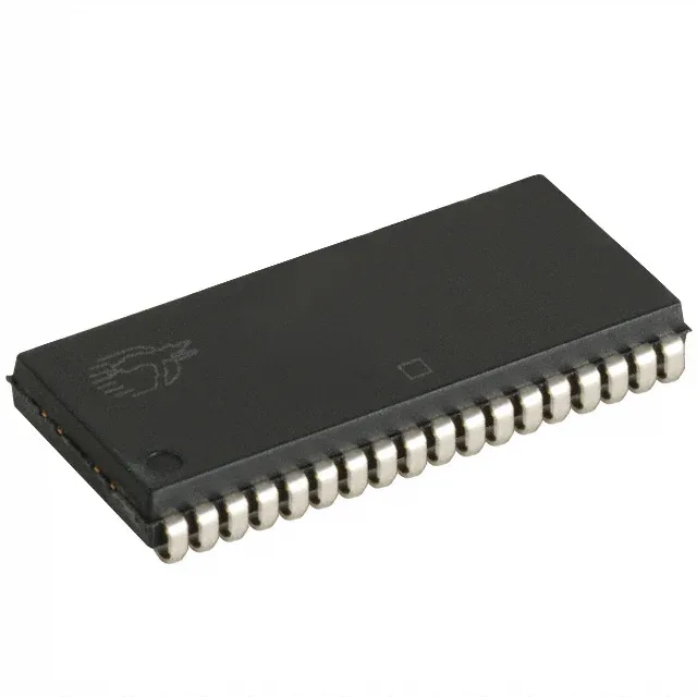
36-SOJ footprint and 10 ns bus timing
The CY7C1049G-10VXI is a 4 Mbit asynchronous SRAM organized as 512K x 8, accessed via a parallel bus with a 10 ns access time — this sets the memory controller's hold-time budget and limits the bus speed to roughly 50 MHz in a typical synchronous read cycle. Housed in a 36-SOJ (Small Outline J-lead) package, 0.400-inch body width, the footprint is a legacy surface-mount form factor that requires a 1.27 mm pitch solder pad layout on the PCB. Operating from a 4.5 V to 5.5 V supply rail, this SRAM is designed for 5 V logic environments — it will not operate from a 3.3 V or 2.5 V bus without a level translator.
Industrial temperature grade and supply
Rated for -40°C to 85°C ambient (TA), the part suits outdoor telecom, industrial control, and base-station equipment where the enclosure sees temperature swings beyond the commercial 0-70°C band. The write cycle time matches the read access at 10 ns — the same bus timing applies for both read and write operations, so the memory controller does not need separate timing parameters for each direction. ROHS3 compliant — no lead, mercury, or restricted phthalates per the current exemption list.