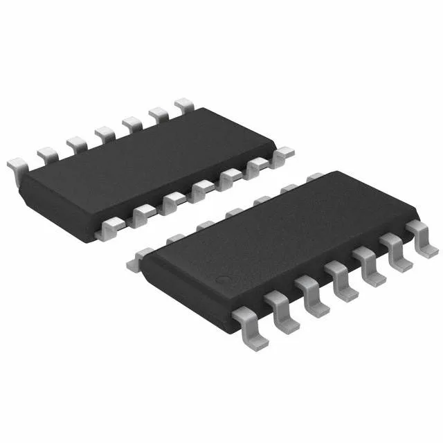
What the open-drain output means for your bus
The 74HC03D is a quad 2-input NAND gate where each output is an open-drain NMOS transistor rather than a standard push-pull stage. This means the output can only sink current to ground — it cannot source current. The high-level output state is achieved by an external pull-up resistor tied to whatever voltage rail the downstream logic needs, up to the 6V supply limit of the device. Open-drain outputs let you wire-AND multiple gate outputs onto a single shared line — any gate that pulls low forces the line low. This is the standard way to implement a shared interrupt or status bus without external OR-gate logic. The pull-up resistor value sets the rise time; for a 50 pF load at 5V, a 1 kΩ resistor gives roughly 50 ns rise time, while a 10 kΩ resistor stretches it to 500 ns.
The 1 µA max quiescent current means it adds negligible power draw in battery-powered or always-on circuits. Propagation delay is 13 ns typical at 6V with a 50 pF load. At 3.3V the delay increases to roughly 20 ns — still fast enough for most control and status logic running below 10 MHz. The 5.2 mA sink current per output drives standard TTL loads and CMOS inputs directly when the pull-up resistor is sized correctly.
The same PCB layout accepts the 74HC08D (AND gate), 74HC02D (NOR gate), or 74HC05D (hex inverter with open drain) without a board spin — all four devices share the same SOIC-14 pinout and supply range. Surface-mount assembly with Tape & Reel or Cut Tape packaging. No thermal pad or exposed paddle — standard FR-4 with 0.5 oz copper handles the thermal dissipation.
No minimum order quantity beyond the reel increment for Tape & Reel orders.