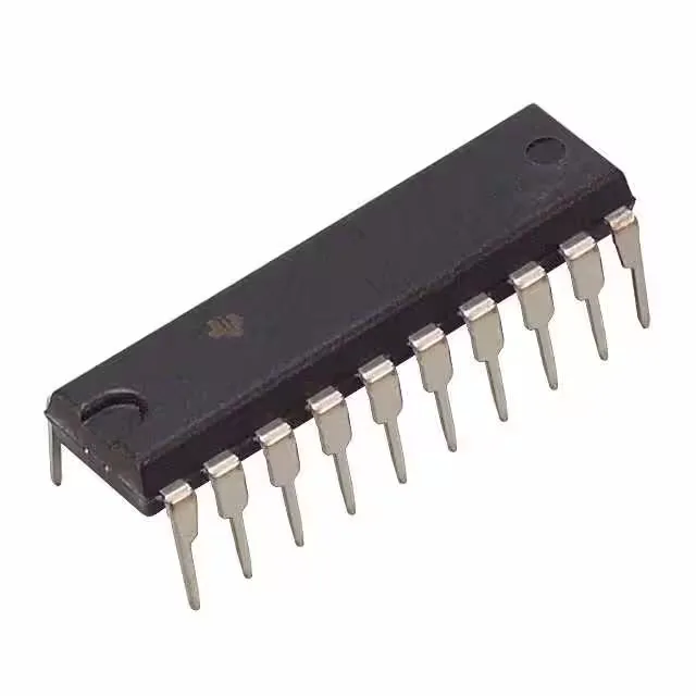
Dual 4-bit inverting buffer with 3-state outputs
Each of the two elements buffers four bits, with a combined output drive capability of 32 mA source and 12 mA sink per output. The 3-state outputs allow the device to be connected directly to a shared bus without contention when the output enable is deasserted.
Output drive and fan-out for bus and signal-line applications
The 32 mA source / 12 mA sink rating sets the fan-out limit for driving standard TTL loads or multiple CMOS inputs. At 5 V VCC, each output can drive up to 32 mA into a terminated transmission line or a bank of logic inputs; the 12 mA sink handles standard LSTTL loads. For a 50 Ω backplane or a heavily loaded address/data bus, this drive level ensures clean edge rates without external line drivers. The inverting function means this part is chosen where the bus polarity needs flipping — common in memory address decoding or control signal inversion where a non-inverting buffer would create a logic error.
At the low end, 4.5 V still guarantees the output drive specs; at the upper end, 5.5 V is the absolute maximum before the BiCMOS process risks breakdown.