Typical applications include memory-address buffering, backplane driving, and control-signal inversion in industrial control, telecom line cards, and general-purpose digital systems operating from a 5 V supply rail.
Drive strength and bus loading — 32 mA source, 64 mA sink
The output drive capability of 32 mA high and 64 mA low is the headline rating that determines how many loads this buffer can drive on a backplane or memory bus. The asymmetric sink-to-source ratio is typical of BiCMOS output stages optimised for driving capacitive loads on the falling edge, where most of the transient current is drawn. For a heavily loaded 16-bit bus, stack the total capacitive load against the propagation delay derating; at 50 pF per line the 64 mA sink edge rate keeps the signal within a 5 V TTL noise margin.
Supply and temperature — 5 V industrial range
The 5 V-only supply means it is not a candidate for mixed-voltage 3.3 V/5 V buses without level translation; for that, the 74LVTH family (e.g. SN74LVTH16245ADGVR) operates down to 2.7 V.
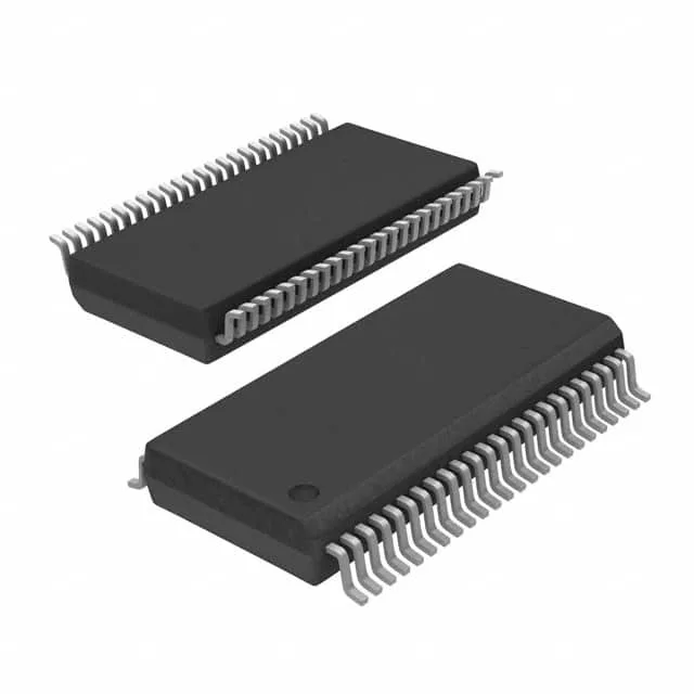
Footprint — 48-SSOP, 300 mil body
This is a surface-mount footprint distinct from the narrower 48-TSSOP (6.1 mm) or the wider 48-SSOP (10.3 mm) variants used in other 74ABT bus functions. Verify the PCB land pattern against the package drawing before committing the layout; the 0.635 mm pitch is standard for SSOP and does not require via-in-pad.
It is a current-production part, not subject to last-time-buy or end-of-life notices at this time.