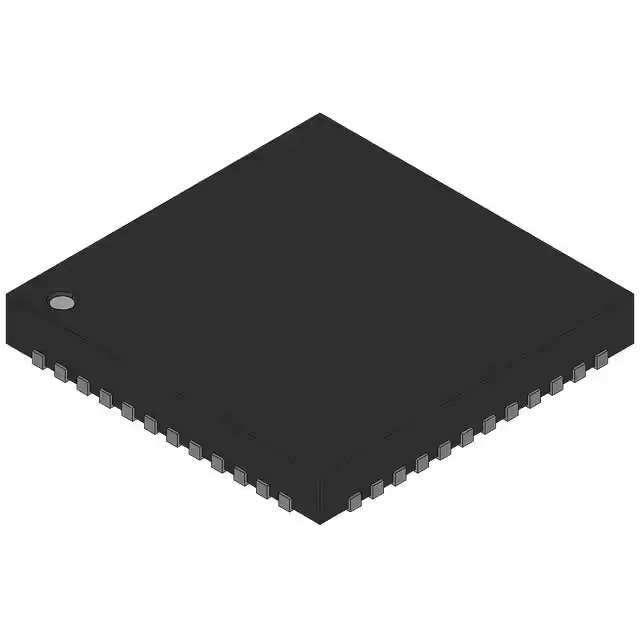
Clock conditioning with the integrated PLL
The LMK04002BISQX/NOPB: This is a Clock Conditioner — a single-chip solution that cleans jitter from a reference clock and synthesizes multiple output frequencies. The integrated PLL (Yes) is the core of the jitter-cleaning loop, locking to the input and regenerating the output with lower phase noise. The maximum output frequency reaches 1.75 GHz, making it suitable for conditioning clocks in high-speed ADC/DAC sampling, FPGA transceivers, and SERDES reference chains.
I/O standards and fanout
The input accepts LVCMOS, LVDS, or LVPECL levels — covering the three most common reference clock formats in digital and RF systems. The outputs are available as LVCMOS, 2VPECL, or LVPECL, giving the system architect flexibility to drive multiple logic families from one device. With a 2:7 input-to-output ratio, one reference clock fans out to seven conditioned outputs. The differential capability on both input and output sides means the device can drive long backplane traces or cables with the signal integrity that differential signalling provides.
The supply voltage is a tight 3.15 V to 3.45 V — the internal PLL and VCO are sensitive to rail noise, so a clean 3.3 V rail with adequate decoupling is expected. The 48-WFQFN package with exposed pad (7x7 mm) requires a thermal pad on the PCB to conduct heat away from the die. The pad should be connected to the ground plane with multiple vias, as the thermal and electrical reference share the same node.