Active production — BOM-fit decision
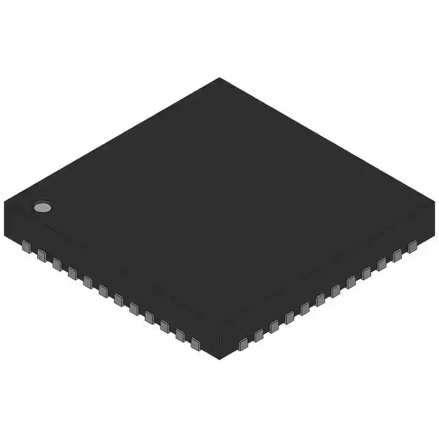
The LMK03001DISQE/NOPB: This is a Clock Conditioner — it cleans jitter and reshapes clock edges from an input source, not just a simple buffer or fanout. The part accepts LVCMOS, LVDS, or LVPECL inputs and delivers LVDS or LVPECL outputs across a 1:8 fanout ratio.
1.57 GHz ceiling and the jitter budget
The 1.57 GHz maximum frequency sets the upper bound for the serial data rate this conditioner can support — for a 10 GbE link using a 156.25 MHz reference, the part operates well within its margin, but a 12.5 Gbps line with a 195.3125 MHz reference approaches the limit. The differential input and output paths (Yes/Yes per the spec) mean the part handles the signal integrity requirements of high-speed serial protocols like PCIe, SATA, and 10GbE without single-ended crosstalk penalties.
Supply rail and thermal management
The 3.15 V to 3.45 V supply range is tighter than a typical 3.3 V ±10% bus — the rail feeding this part needs a low-noise regulator, not a switching supply without post-regulation, to stay inside the window across load and temperature. The datasheet's recommended land pattern should be followed exactly — the exposed paddle is the primary thermal path, and insufficient vias raise the junction temperature above the 85°C operating limit.
Industrial temp grade and deployment context
The single-circuit design (Number of Circuits: 1) means one conditioner per package. For designs needing multiple independent clock trees, each channel requires its own LMK03001 — the 1:8 fanout serves eight downstream loads from one input.