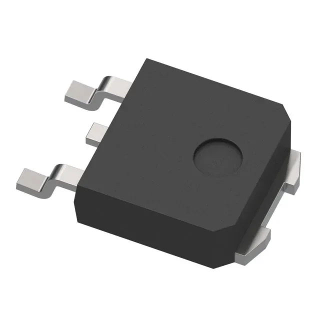
STMicroelectronics STD15N50M2AG — Discrete Semiconductors

STD15N50M2AG N-Channel 500V 10A DPAK MOSFET, AEC-Q101

MPNSTD15N50M2AG
Active

STMicroelectronics STD15N50M2AG, Automotive AEC-Q101 MDmesh M2 N-Channel MOSFET, 500V Vdss, 10A Id, 380mOhm Rds(on), DPAK (TO-252), Tape & Reel.

$1.9300Ref. price · indicative, final on quote
PackagingTO-252-3, DPak (2 Leads + Tab), SC-63
RoHSROHS3 Compliant
SeriesAutomotive, AEC-Q101, MDmesh™ M2
Independent supplier — new & surplus stockAuthenticity-screened · ESD-safe packingListing updated Aug 2026

Specifications

STD15N50M2AG specifications
ParameterValue
SeriesAutomotive, AEC-Q101, MDmesh™ M2
FET typeN-Channel
MountingSurface Mount
Drain to source voltage500 V
Drive voltage (Max rds on, min rds on)10V
Current - continuous drain (Id) @ 25°C10A (Tc)
Power dissipation85W (Tc)
Operating temperature-55°C~150°C(TJ)
PackageTape & Reel (TR); Cut Tape (CT)
Vgs±30V
TechnologyMOSFET (Metal Oxide)
CaseTO-252-3, DPak (2 Leads + Tab), SC-63
Vgs(th) (Max) @ id4V @ 250µA
Rds on (Max) @ id, vgs380mOhm @ 5A, 10V
Gate charge (Qg) (Max) @ vgs13 nC @ 10 V
Input capacitance (Ciss) (Max) @ vds530 pF @ 100 V

Product details

Parametric fit for the BOM: what each rating means

The STD15N50M2AG: The 500 V Vdss rating provides a 1.5× derating margin against a 320 V DC bus (typical for 230 VAC input PFC stages) and comfortably handles the 400 V bus in single-phase automotive inverters. Input capacitance Ciss of 530 pF at 100 V drain-source sets the switching transition time. Driving the gate from a 10 V source through a 10-ohm resistor yields a turn-on delay of about 5 ns — fast enough for 200 kHz hard-switching without excessive ringing when the layout keeps the gate loop tight. The ±30 V maximum gate-source voltage gives headroom for gate-drive transients that overshoot the 10 V nominal drive, common in automotive environments with inductive kickback from the load.

Active production, AEC-Q101 qualified

Supplied in Tape & Reel (TR) or Cut Tape (CT) formats for pick-and-place. The DPAK (TO-252) footprint is standard — 2 leads plus tab, with the exposed drain pad on the bottom for thermal dissipation through the PCB.

Frequently asked questions

What is the closest functional alternative to STD15N50M2AG — does STD13N60M2 drop in without rewiring?

The STD13N60M2 (600 V, 11 A, 380 mOhm) shares the same DPAK footprint and AEC-Q101 qualification, but its higher voltage rating (600 V vs 500 V) and slightly different gate charge (17 nC vs 13 nC) mean the gate-drive timing and switching losses shift. The 380 mOhm on-resistance matches at the same 10 V gate drive. Electrically it can substitute in a 500 V circuit with margin, but the gate-drive circuit should be re-verified for dV/dt immunity. No rewiring is needed — same pinout and package.

How do I get current pricing and availability for STD15N50M2AG?

Submit an RFQ through this listing.