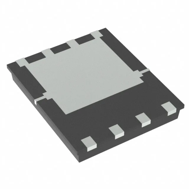
Renesas Electronics RJK1575DPA-00#J5A
Technical Documents PDF / CAD
RoHS Compliant · Lead-Free EIA-481 Standard

RJK1575DPA-00#J5A N-Channel MOSFET, 150V, 25A, WPAK(3F)

MPN RJK1575DPA-00#J5A
End of Life Spot Stock · 24-48h Dispatch 100% Original Sealed

Renesas RJK1575DPA-00#J5A N-Channel MOSFET, 150 V drain-source, 25 A continuous drain at 25°C, 48 mOhm Rds(on) at 12.5 A, 10 V, WPAK(3F) 5x6 surface-mount package, Tape & Reel.

In Stock: 6,000 pcs
MOQ: 1 pcs
Logistics: DHL / FedEx DAP (Global Express · 3-7d) Russia & CIS DDP (Door-to-Door Cleared)
Dispatch: Shenzhen / HK
Unit Price (USD)
$1.59 / pc
Direct Purchase Ready
Volume Pricing Breaks Confirmed upon quotation
1+ pcs
$1.59
10+ pcs
$1.43
30+ pcs
$1.30
100+ pcs
$1.17
500+ pcs
$1.09
1,000+ pcs
$1.03
Working on a production BOM or have a target unit price? Submit Target Price
Buy Now

$1.59 / ea

6,000 in stock — maximum per order · 3–4 days lead time

$1.43 / ea from 10 pcs

Upload Full BOM List
[SPEC] Essential Parameters Snapshot Full Specifications (14)
Package / Case 8-PowerVDFN
Output / Current 150 V

Full Technical Specifications

14 Parameters
RJK1575DPA-00#J5A specifications
Parameter / AttributeSpecification / Value
FET typeN-Channel
MountingSurface Mount
Drain to source voltage150 V
Drive voltage (Max rds on, min rds on)10V
Current - continuous drain (Id) @ 25°C25A (Ta)
Power dissipation65W (Tc)
Operating temperature150°C (TJ)
PackageTape & Reel (TR)
Vgs±30V
TechnologyMOSFET (Metal Oxide)
Case8-PowerVDFN
Rds on (Max) @ id, vgs48mOhm @ 12.5A, 10V
Gate charge (Qg) (Max) @ vgs37 nC @ 10 V
Input capacitance (Ciss) (Max) @ vds2200 pF @ 25 V
[DESK] Shenzhen Spot Allocation · 2h Response

Need Immediate Spot Stock or Shortage Allocation for RJK1575DPA-00#J5A?

Factory lead times blocking production? We lock verified brand-new original stock in Shenzhen within 2 hours.

Quote SLA 2 Hours
[01] Emergency Shortage 24-48h Shenzhen Dispatch

Direct access to Shenzhen floor inventory, franchised allocation buffers, and factory bonded stock to resolve line-down shutdowns.

[02] Industrial Packaging Tape & Reel / Tray / Tube

Standard factory-sealed packaging compliant with EIA-481 standards for automated high-speed SMT pick-and-place lines.

[03] WhatsApp QC Proof 45x Microscope QC Photos

High-resolution photos of original reel labels, 2D DataMatrix, and pin coplanarity sent via WhatsApp/Telegram before you release wire payment.

● USD Wire Transfer (SWIFT T/T) · DAP Express / DDP Delivery

Technical Details & Description

150 V N-Channel MOSFET in a 5x6 WPAK(3F) package

It is built on a standard metal-oxide semiconductor process and comes in an 8-PowerVDFN package — the WPAK(3F) variant with a 5x6 mm footprint and an exposed thermal pad for heat sinking into the PCB. Gate charge totals 37 nC at 10 V, and input capacitance is 2200 pF at 25 V drain-source — numbers that matter for the gate-driver sizing and switching-loss calculation in a 48 V or 72 V bus converter.

The 150 V drain-source rating gives headroom for 48 V and 72 V nominal rails — a 48 V bus sees transients up to 60 V, so the 150 V ceiling leaves margin without oversizing to a 200 V device. The 25 A continuous rating at 25°C case is the headline number, but the real-world current is limited by the 65 W power dissipation ceiling and the PCB's ability to sink heat from the exposed pad. Derate for ambient temperature and switching losses. The 48 mOhm Rds(on) at 10 V gate drive means conduction loss at 12.5 A is about 7.5 W — well within the 65 W dissipation limit at 25°C case, but junction temperature rise will cut into that margin at higher ambient. The 37 nC gate charge is moderate; a typical gate driver with 1 A peak source/sink can switch this FET in the 100–200 kHz range without excessive crossover loss.

The 5x6 mm pad needs a thermal land pattern with multiple vias to the inner ground plane — the datasheet's recommended footprint is the starting point, and the via count and copper area set the effective RthJA.

Frequently asked questions

What is the closest functional second-source for the RJK1575DPA-00#J5A?

The NP179N055TUK--AY is an automotive-grade N-Channel MOSFET with a 55 V drain-source rating, 180 A continuous current, and 1.75 mOhm Rds(on) — it is not a pin-compatible or direct replacement for the 150 V / 25 A RJK1575DPA-00#J5A. The voltage and current classes differ significantly, so treat it as a different design target rather than a second source.

RJK1575DPA-00#J5A
Verified Allocation
Quote